You will not find any commercial product: both the topology, and the name "circlomos" are my creations.Unfortunately I find only RF amplifier devices there (lowest frequency: 10 KHz).
It would take the colloquial term of the Circlomos to find a comparable commercial product respective commercial brand about google.
There are other makers of lab amplifiers: in addition to R&S (or was it W&G? I always mix them up), there also is (was?) a french maker, but the name of the brand escapes me for the moment.
I have spotted two mistakes on your version of the schematic: D5 is reversed, and R12 should be 3.9K.Here now the second PDF attachement - same conditions than my first attachement except idle current through the output stage: now only 96mA (M1) and 133mA (M2) and much more bad THD results (as always observe by reducing the idle current):
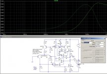
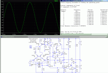
1) schematic for damping factor over frequency
2) AC-Analysis (damping factor over frequency)
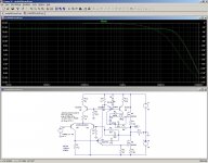
3) AC Analysis - not show !! (normally frequency response)
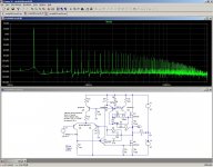
4) Fourier Analysis lin 10 KHz (THD)
5) Fourier Analysis log 10 KHz (THD)
6) Fourier Analysis log 100 KHz (THD)
7) Fourier Analysis lin 100 KHz (THD)
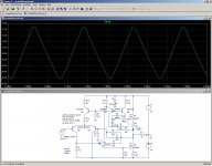
8) Transient Analysis 1 MHz
9) Transient Analysis 10 MHz
10) schematic (normally frequency response)
And now the clipping behavior (10-times higher input voltage for theoretical 100Vss output)
1) schematic
2) Voltage output at load - 8 ohms
3) Gate signal current M1
4) Gate signal current M2
5) Base signal Current Q1
6) signal Current R12
Simulation results for the distortion are to be taken with a pinch of salt: they give the right order of magnitude, but they are rarely spot on: in ~80% of the cases, I find the actual, measured value is somewhat higher than simulated, in ~10% of the cases, it is better, and the remaining 10% are about right.About number 2 to 7 can be seen clearly that the p-spice models do not perfect or my simulation program "Circuit Maker" is overtaxed. What about the simulation results in this case with your LTspice?
One or two things to remember about this amplifier:
It's cheap, it's N, it's dirty,
This design is optimized to be simple, cheap, robust, stable and energetically efficient. If there is still room for linearity, so much the better...Crude, but effective
There are a number of identified causes of non-linearity: one is the folded cascode: not all the current from the NPN circlo phase shifter is transferred by the PNP to the upper MOS (because the low-value emitter resistor R9 shunts part of the current), meaning the circlo symmetry of the driver stage is not perfect.
Another is the switching action of D1 when the threshold-shifter enters the "hold" mode: this removes some current from the drive to M1 and causes distorsion.
For this reason, the current through D1 (hence D2) is kept minimal.
The low bias current is also required for the subsequent versions including the autobias: operating the zener in a "soft" part of its characteristic gives more compliance to the control.
This should answer your question:
Note that these are deliberate choices, which are not inherent to the topology itself: it would be easy to improve by including a transistor here and there, and wasting a little swing in the output voltage.Independend of this - I don't understand the value of R12 (3K9) in your circuit - there are only 0,2mA current flow through the zener.
Everyone is free to make the improvements he judges necessary, and come up with its own version: Circlomanen has done so, albeit in the opposite direction.
Thank you very much for your replies in post #41. I agree with all except in case of D5: When D5 would be a zener diode it would be the wrong direction (please note: Zener diodes are bidirectional diodes, one direction the zener voltage, the other direction approx 0V65 - 0V7 - like a normal diode) But I chose a normal diode, i. e. an unidirectional diode. So the choiced direction of me isn't wrong.
Regarding the clipping behavior I wrote the following:
"About number 2 to 7 one can be seen clearly that the p-spice models do not perfect or my simulation program "Circuit Maker" is overtaxed. What about the simulation results in this case with your LTspice?"
But I mean number 3 to 7 of the second pdf !!! - only the four different AC current transient signals (transient analysis)
I get the mentioned current signals through introducing current sense resistors in the gate line, that have very low values without influence of the other parameters.
What show LT-Spice here in case of clipping? That would be highly of interest, because thereby I can identify and compare the character of the simulation work (and perhaps different p-spice parameter of the MOSFETs)
Regarded the idle current control - what about the voltage source solution of
circuit diagram about
http://www.amplimos.it/images/N-CH1.JPG
original article: Original article: "Better Audio from non complements?" from Bengt Olsson (B. Olson?)
Electronics World + Wireless World, December 1994 page 988
In your topology this voltage source must be in serial of R13 - I think.
At best an completly independend power supply include individual main transformer winding especially for this. As I know, ASKA uses this topology
weblink: Amplifier Kits - Audio Amplifier Modules - MOSFET Amps
For detail improving this articles could be also helpful:
http://www.ant-audio.co.uk/Theory/N-channel D-MOSFET output stage with improved linearity.pdf
and Ollsons attached topology from aussieamplifiers.
I still missed statements from Mr. Nelson Pass and Alex Nikita (X-PRO) Perhaps the title of this thread can't assume this interesting topology, and therefore this thread doesn't open the most here
Attachments
Last edited:
Interesting reasoning.Thank you very much for your replies in post #41. I agree with all except in case of D5: When D5 would be a zener diode it would be the wrong direction (please note: Zener diodes are bidirectional diodes, one direction the zener voltage, the other direction approx 0V65 - 0V7 - like a normal diode) But I chose a normal diode, i. e. an unidirectional diode. So the choiced direction of me isn't wrong.
You must have received a jesuit education.
You can always reverse a zener in any circuit... but then the circuit will behave differently. Similarly, you could argue that BJTs can have their emitter and collector swapped: they also work in the reverse direction, only with a reduced beta.
Reversing D5 disables the threshold level shifter. If you really want to do that, you can in fact remove it completely, as well as C3, D1, R13, D6, Q6, R12.
You then have to halve R9, to rebalance the circlo operation. It will also work, but the positive excursion will be limited, as in your simulations.
If you insist on simulating "your" circuit, it makes little sense to try to make comparisons.Regarding the clipping behavior I wrote the following:
"About number 2 to 7 one can be seen clearly that the p-spice models do not perfect or my simulation program "Circuit Maker" is overtaxed. What about the simulation results in this case with your LTspice?"
But I mean number 3 to 7 of the second pdf !!! - only the four different AC current transient signals (transient analysis)
I get the mentioned current signals through introducing current sense resistors in the gate line, that have very low values without influence of the other parameters.
What show LT-Spice here in case of clipping? That would be highly of interest, because thereby I can identify and compare the character of the simulation work (and perhaps different p-spice parameter of the MOSFETs)
Interesting. I was not aware of that one. Basically, it is the Thevenin interpretation of the circlo concept (virtual complements). I went the Norton way.Regarded the idle current control - what about the voltage source solution of
circuit diagram about
http://www.amplimos.it/images/N-CH1.JPG
I was aware of this one, and I based my design on this concept. I find it powerful and interesting, and I found disappointing the harsh judgement made by D. Self about it.original article: Original article: "Better Audio from non complements?" from Bengt Olsson (B. Olson?)
Electronics World + Wireless World, December 1994 page 988
See Norton/Thevenin above.In your topology this voltage source must be in serial of R13 - I think.
That's my way of doing things:Perhaps the title of this thread can't assume this interesting topology, and therefore this thread doesn't open the most here
 never take anything too seriously
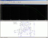
You have a very interesting amp. The closest commercial equivalent would be this: Model 6552-1A 100 watt Solid State Audio Amplifier used for testing power line noise immunity. Again durability is paramount in these things. Which also brings tradeoffs in distortion/noise versus indestructability. For sheer bandwidth the amps from Krohn Hite are the most equivalent Krohn-Hite Corporation - A Leading Manufacturer of Test and Measurement Instruments Since 1949. I have one thats broken. I have been reluctant to service it since the supplies are +/- 200V making it rather hazardous to poke around in. Some long weekend when nothing else is more pressing. . .
Your solution is much cheaper and could be packaged as a disposable module for a commercial market.
Your solution is much cheaper and could be packaged as a disposable module for a commercial market.
Thanks for the pointers. That's exactly the kind of product I wanted to give as examples to tiefbassuebertr.You have a very interesting amp. The closest commercial equivalent would be this: Model 6552-1A 100 watt Solid State Audio Amplifier used for testing power line noise immunity. Again durability is paramount in these things. Which also brings tradeoffs in distortion/noise versus indestructability. For sheer bandwidth the amps from Krohn Hite are the most equivalent Krohn-Hite Corporation - A Leading Manufacturer of Test and Measurement Instruments Since 1949. I have one thats broken. I have been reluctant to service it since the supplies are +/- 200V making it rather hazardous to poke around in. Some long weekend when nothing else is more pressing. . .
Your solution is much cheaper and could be packaged as a disposable module for a commercial market.
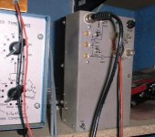
The incarnation of an early version of mine does bear a "family likeness" with these products:
Attachments
from post #18 The next variant has a higher loop gain.
This results in a higher feedback factor, and a reduced distortion: the linearity is now around 5 ppm at near-full power (0.0005% dist.)
Other characteristics remain practically unchanged.
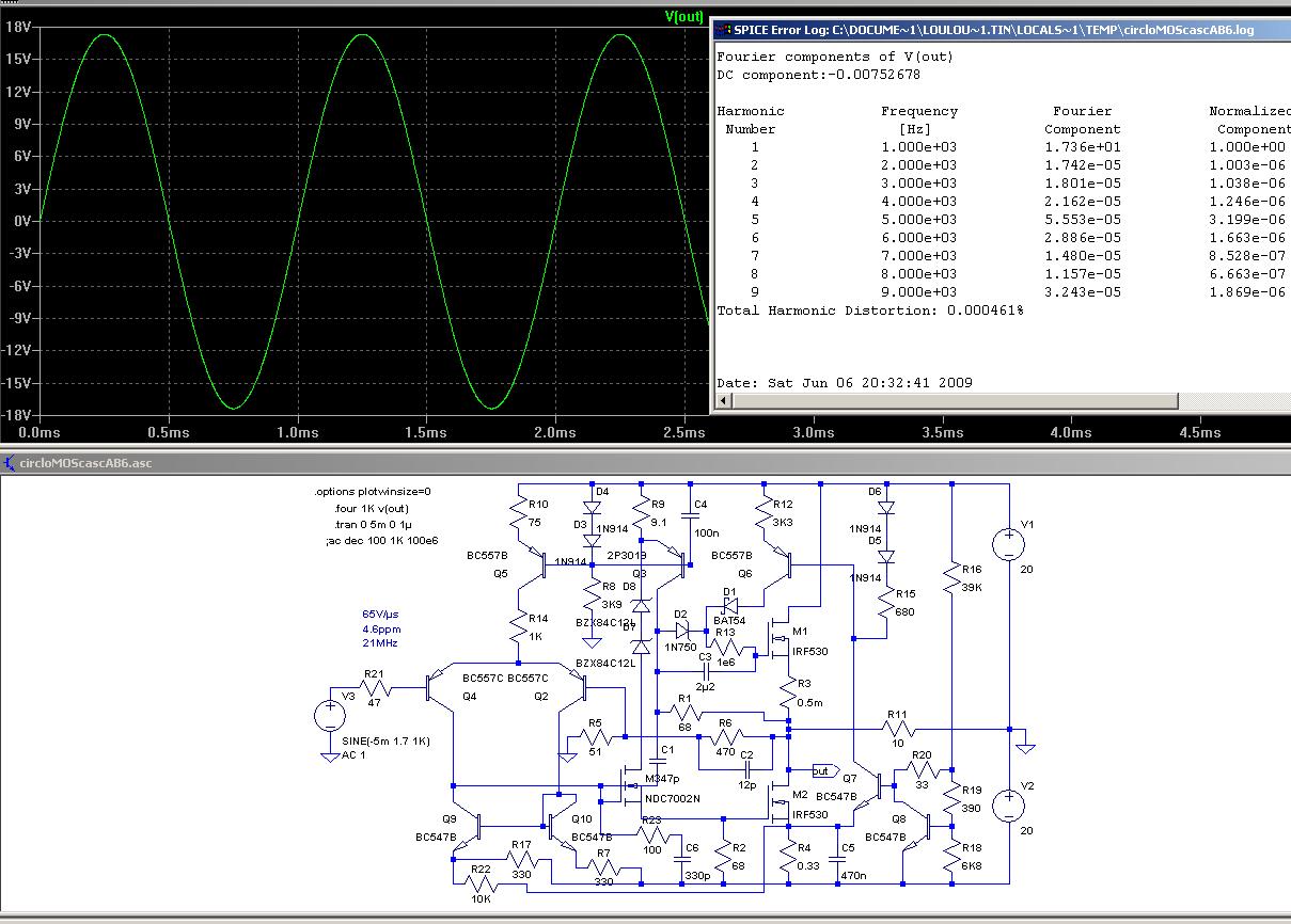
Here my simulation results of this circuit by 10Vss output and 1200mA idle current through the output (slightly modify the comensation to get results):
1) schematic with mentioned dc voltages (set by simulation)
2) AC Analysis (normally frequency response)
3) Fourier Analysis lin 10 KHz (THD) K2: 540uV, K3: 230uV
4) Fourier Analysis log 10 KHz (THD)
5) AC-Analysis (damping factor over frequency)
Unfortunately I don't get the follow diagrams:
Fourier Analysis log 100 KHz (THD)
Fourier Analysis lin 100 KHz (THD) K2: 1130uV K3: 390uV
Transient Analysis 1 MHz
Transient Analysis 10 MHz
Already by 20 KHz I get only error messages (by the introduce of current mirrors in generall - independend of the circuit topology)
The reason is, that my simulations software don't like current mirror's. If I remove the current mirror, then I get all diagrams again. Instead of current mirror I will test the two transistor topology Q6/Q5 of X-Pro in the schematic of first post about
http://www.diyaudio.com/forums/solid-state/122378-cambridge-audio-a3i-repairs-mods.html
You have a very interesting amp. The closest commercial equivalent would be this: Model 6552-1A 100 watt Solid State Audio Amplifier used for testing power line noise immunity. Again durability is paramount in these things. Which also brings tradeoffs in distortion/noise versus indestructability. For sheer bandwidth the amps from Krohn Hite are the most equivalent Krohn-Hite Corporation - A Leading Manufacturer of Test and Measurement Instruments Since 1949. I have one thats broken. I have been reluctant to service it since the supplies are +/- 200V making it rather hazardous to poke around in. Some long weekend when nothing else is more pressing. . .
Your solution is much cheaper and could be packaged as a disposable module for a commercial market.
Thank you very much for this very interesting advices. I have ask there to schematics of their all currently available models of wideband amplifiers.
So far I always assumed that only components (especially electrolytic capacitors and foil capacitors), if they are offered as a typical audio components, are usually not as good as those that are specific made for the industry (e. g. electronic energy systems).
Obviously, this assumption is perhaps sometimes true even by complete amplifier devices, because the necessary "Know How" for military and industry applications must be much more higher than for the ordinary consumers in their audio-hifi stuff.
By the way, the follow website of you
element.us.com
is death
I find it only about
Internet Archive Wayback Machine
e. g.
element
Last edited:
Here my simulation results of this circuit by 10Vss output and 1200mA idle current through the output (slightly modify the comensation to get results):
1) schematic with mentioned dc voltages (set by simulation)
2) AC Analysis (normally frequency response)
3) Fourier Analysis lin 10 KHz (THD) K2: 540uV, K3: 230uV
4) Fourier Analysis log 10 KHz (THD)
5) AC-Analysis (damping factor over frequency)
Unfortunately I don't get the follow diagrams:
Fourier Analysis log 100 KHz (THD)
Fourier Analysis lin 100 KHz (THD) K2: 1130uV K3: 390uV
Transient Analysis 1 MHz
Transient Analysis 10 MHz
Already by 20 KHz I get only error messages (by the introduce of current mirrors in generall - independend of the circuit topology)
The reason is, that my simulations software don't like current mirror's. If I remove the current mirror, then I get all diagrams again. Instead of current mirror I will test the two transistor topology Q6/Q5 of X-Pro in the schematic of first post about
http://www.diyaudio.com/forums/solid-state/122378-cambridge-audio-a3i-repairs-mods.html
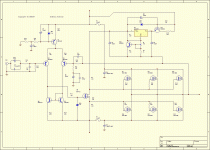
Some remarks about this schematic: it is derived from a very similar version using a BJT as the circlo phase shifter. This variant, using a MOS, M3, is a theoretical exercise, and has not been tested, just simulated.
In addition, the circuit was initially calculated for 20V supplies. I just changed the supplies to 50V "to see what happens", following a request by AKSA, and it happened to operate almost normally, but all this means we are in uncharted territories.
In addition, your schematic shows a number of errors and inconsistencies:
-R3 is a test resistor of 0.5milliohm, not 0.5ohm
-R20 is 33 ohm, not 330
This should result in a much lower Iq. Yet, you get 1200mA in your sim (I had 300mA with the "normal" version)
This is clearly inconsistent (yet your schematic shows that Q8 is in hard saturation)
Now, there remains an obvious inconsistency, and it has to be in your 1N750 model: there is only 63pA passing through it, yet the voltage is 4.55V, almost the nominal voltage.
This means the ideality factor must be unrealistically good, or something similar.
At this level of current, these low-voltage diodes behave like ~short circuits.
This means the ideality factor must be unrealistically good, or something similar.
At this level of current, these low-voltage diodes behave like ~short circuits.
For sheer bandwidth the amps from Krohn Hite are the most equivalent Krohn-Hite Corporation - A Leading Manufacturer of Test and Measurement Instruments Since 1949. I have one thats broken. I have been reluctant to service it since the supplies are +/- 200V making it rather hazardous to poke around in. Some long weekend when nothing else is more pressing. . .
Dou you have also a circuit diagram resp. schematic diagram of this device from the Krohn-Hite Corporation?
I do have the manual. However having it and knowing where it is do not necessarily correspond. I will try to find it over the next few days and scan and post the circuit drawing. There is a lot to learn from them. They have a long history of building wide band amplifiers and a large collection of tricks in the designs to solve problems "waiting for the unwary".
CircloMOS-XQ
Here is another variant of the circuit, where the higher loop gain and resulting lower distortion is achieved by means of a crossquad input stage.
This should please those unhappy with current mirrors.
Note that this is a pure simulation exercise: the circlo topology and the Xquad input have both been validated, but separately.
Some food for thoughts.
Also note that the Xquad is not an easy beast to tame: its input impedance is negative, and it will oscillate unless the source impedance is very nearly zero.
Have fun anyway
Attachments
Im building a small version of this amp today.
Since im using what i have at home, it will be a 5 - 7 watt version using a 19 volts single rail powersupply and two IRF3706 in the output.
Since im using what i have at home, it will be a 5 - 7 watt version using a 19 volts single rail powersupply and two IRF3706 in the output.
An externally hosted image should be here but it was not working when we last tested it.
An externally hosted image should be here but it was not working when we last tested it.
Slowly making some progress.
I found a LED that have a 1,72 v drop when running 0,7 mA through it. It should be perfect bias to the IRF3706.
Interesting.
I am curious to see the results with a rather large, high conductance, high capacitance device like the 3706.
The IRF530 and BUK453 I used for the tests have a lower gfs and a third of the capacitances.
Have you seen the message about the compensation?
http://www.diyaudio.com/forums/soli...-n-its-dirty-its-circlomos-5.html#post2008665
Anyway, with the 3706, other values might be required.
Good luck and good fun!
Have you seen the message about the compensation?
Yes, i have read that. I have read this thread 10 times all the way through...

I hope i understand this one... I will try without compensation first.
I hope i can hear if there is any serious problem with it. I dont have any scope or anything. Maybe i will place a 100 pF cap from the collector to the base on the phasesplitter/vas transistor. A millercap.
This is just a test. I use what ever i have at home. I hope it will work, i do think your amp is a novel design. I like the simplicity of it.
Johannes.
- Status
- This old topic is closed. If you want to reopen this topic, contact a moderator using the "Report Post" button.
- Home
- Amplifiers
- Solid State
- It's cheap, it's N, it's dirty, it's.... The CIRCLOMOS!!!