Hi,
I'm working on an amp with a CFP output stage and I'm having some issues with the stability of the OPS, most likely due to the high fT of the output transistors (I'm sure this isn't down to inadequate dominant-pole compensation - the OPS is taking off by itself).
The output transistors are Sanken 2SA1295/2SC3264 (2 devices in parallel with 0R1 emitter ballast resistors), and the drivers are 2SB649 and 2SD669.
After some experimentation, I'm settling on 150R in parallel with 2n2 between the base and emitter of the output transistors - without the caps there I'm able to induce bursts of oscillation at about 10MHz on the output transistor bases (those sanken transistors are really something else...).
As it is, the amp is now completely stable, but I'm not convinced I've got to the bottom of the problem and that I'm getting the best performance from the OPS. Are there any design formulae / rules of thumb I can use to check the values of the output transistor base-emitter resistors and the driver base-stopper resistors?
I'm sure it must be related to the VAS current drive and the relative HFE of the driver and output transistors, but I'm stuck cutting-and-trying when I want to be calculating")
Any advice much appreciated.
Cheers..
I'm working on an amp with a CFP output stage and I'm having some issues with the stability of the OPS, most likely due to the high fT of the output transistors (I'm sure this isn't down to inadequate dominant-pole compensation - the OPS is taking off by itself).
The output transistors are Sanken 2SA1295/2SC3264 (2 devices in parallel with 0R1 emitter ballast resistors), and the drivers are 2SB649 and 2SD669.
After some experimentation, I'm settling on 150R in parallel with 2n2 between the base and emitter of the output transistors - without the caps there I'm able to induce bursts of oscillation at about 10MHz on the output transistor bases (those sanken transistors are really something else...).
As it is, the amp is now completely stable, but I'm not convinced I've got to the bottom of the problem and that I'm getting the best performance from the OPS. Are there any design formulae / rules of thumb I can use to check the values of the output transistor base-emitter resistors and the driver base-stopper resistors?
I'm sure it must be related to the VAS current drive and the relative HFE of the driver and output transistors, but I'm stuck cutting-and-trying when I want to be calculating
Any advice much appreciated.
Cheers..
I haven't built high performance high power output stages but the analysis or realistic simulation is problematic
the feedback loop requires the more advanced Tain loop gain probe or Middlebrook GFT tools to measure loop gain
at 10 MHz wiring parasitics can be significant - even package parasitics should be considered
both drive and load impedance at high frequencies are important - base stopper, interstage Zobel and output inductor and Zobel can help establish known input and output impedance even with relatively high load variability
another place for compensation of the local loop is to add series R between the output and the input Q emitter - this position is the feedback R in the ~equivalent CFA op amp and controls the dominant pole of the local loop (with the C seen at the output Q base node)
Last edited:
at 10 MHz wiring parasitics can be significant - even package parasitics should be considered
Indeed. I don't think spice simulation is at all useful here.
The output devices in my design are wired off the amplifier PCB.
I'm using longer wires for testing than I plan to use for the final build (by about 2x), but IMO a well behaved amp should have enough stability margin to cope with that.
I chose the output devices primarily for Hfe linearity versus Ic; their high fT is just causing trouble so I'm trying to reduce it (hence the 2n2 caps).
I like the idea of adding resistance between the driver emitter and the output (currently the driver emitter is connected to the output collectors) - I can see how this would work.
Thanks for the comments
Forgive the dumb question, but why use a CFP? OK, so you need some gain coming out of th e VAS, or you want to make use of all the voltage you have available, but these things are really, really problematic. Better to supply the VAS off a slightly higher voltage and up your output supply voltage up a bit and just use a good old triple.
27pf CoB for the driver, ouch!. Thats the big problem, this will cause much Phase Shift in itself hence the oscillation problems at 10 Mhz, the Gbw limit of the OP devices. Without slugging the driver with a 33pf and higher miller cap I would try and find a low Cob replacement , under 10pf, or go with a triple. Is it running Class A or A/B?, if A/B the EF will be much easier to implement without the crossover nasties which could also explain the random bursts you describe. Once all is working well, the sound of a Cfp is astounding!
Colin
Colin
Hi there,
Thanks for all the comments. I *will* make the CFP work, but I would really appreciate any further help with device selection and analysis
So my thinking behind the device selection - I chose the output transistors based on their high fT (~60MHz), nice flat beta response and good SOA; I doubled them up so that I stay on the flattest part of the beta/Ic curve right up to maximum power, and to keep the VI limiting from needing to kick in anywhere near to normal levels.
I then chose the drivers to have higher fT (~140MHz) than the output devices. It was actually pretty hard to find transistors that have high enough fT and large enough SOA; the 669/649 looked to be a bit special. I think because the output transistors are common emitter and are 'controlled' by the 100% feedback through the drivers, the GBP of the driver has to be higher than the output transistors; this makes me wary of adding a cap between B and C of the drivers.
I'm going to spend a bit of time in spiceworld to see if I can get a better understanding of how to compensate this thing; it must be possible to get the outstanding beta/Ic properties of the output transistors without the stability problems.
Cheers,
cfp stability
So the latest CFP output I have built uses on 2 MJL1302 and 2 MJL3281a devices driven by single MJE15033/15035.
I did not need compensation, but here are some of the tricks I employed to ensure stability of the OP. ( though I have footprints )
For the input device I degenerated the gain to 22X. More than 50X seems to cause an undue increase in sensativity.
The bases of the power devices have about 10Ohm resistors on them. These are there for precisely the same reason as MOSFET gate stopper resistors - to slug out the trace impedance and input capacitance.
The Power device emitter degridation resistors are 0.2.
Decoupling caps. Get some rail decupling caps CLOSE to the the OP stage. CFPs are sensative to PSU impedance at the top end of their operating frequency.
I have 19mm of trace from any resistors to the pins, and that is at the edge of my comfort zone.
--
To the question of why...
The gain pair with local feedback seems to provide a VERY pleasing sound when it works.
It can be painfull, but the true artist needs some pain. ;-)
Be warned that when they oscilate they can do so in a violent manner.
Brian
Hi Brian,
Thanks for your comments.
I was considering increasing the output resistors from 0R1 to 0R22 or 0R33 as this will increase the voltage fed back to the driver emitter; sounds like it worked for you so I'll definitely try it. Reducing the local loop gain of the stage and flattening out the frequency response will also help greatly. I suspect that this will be the final fix.
As I said earlier, I want to understand the root cause and stabilise the stage intelligently; I don't believe in just playing with things until they work. My aim is to have something that's fairly tolerant of layout/construction and has a well defined stability margin.
As for oscillating violently - yes, I can vouch for that! I would definitely not recommend the CFP topology to anyone without a decent scope, variable current-limit PSUs and probably a distortion analyser too. You're also right that something worth having is worth working at and suffering for
Cheers,
So there was a comment on the simulating the output.
My practice there is that if there is any hint of a rise in gain at turnover you will have parts flying around the lab.
The very nature of a cfp is that the transistors have different frequency abilities EVEN if they are the same device. And this is due to one working as a V gain device, and one working as a iI gain device.
This means that at some operating point there will be a phase imbalence between them.
And phase imbalence causes a reduction of stability margin - and at some point that is large enough to causes oscillation.
We work with this in the rest of the amplifier, we band limit the input and put HF limiting in the input and VAS stage.
This is normal.
But for some reason people think that the output stage should be immune to such thought processes.
Just my soap box.
--
But from an understanding point of view if you have an L meter measure the trace and wire inductance for all the connections and plug them into the simulation model. The first time I did this it was 'illuminating'.
Brian
mmmhh..
a ferrite bead in series with the base of the power transistor could be usefull. But you need to find the right one. At low frequency it has a zero impedance and you can choose the right ferrite bead with a peak at the frequency where it oscillate. But it needs a lot of testing.
a ferrite bead in series with the base of the power transistor could be usefull. But you need to find the right one. At low frequency it has a zero impedance and you can choose the right ferrite bead with a peak at the frequency where it oscillate. But it needs a lot of testing.
Atomicplayboy,
I don`t want to discourage you, but... in my humble estimation, the chances of a successful outcome are in the region of zero %.
Well, I feel that I'm making some progress with the analysis, and I'm learning more about the intricacies of the CFP configuration... And of course I now want to prove Lumba wrong
The stage consists of two back to back common emitter amplifiers (now that I look at it more closely...) so the open-loop gain is very large, and with 100% feedback applied we have about the worst case for stability. So to stabilise, I need to either reduce the feedback factor, add an LF pole or reduce the open-loop gain. The first option will add voltage gain to the stage which I don't want to do; the second will complicate things when incorporated into an amplifier with global feedback and dominant-pole compensation, so I'm looking at reducing transconductance of the transistors using emitter degeneration.
This is not straightforward since degeneration is based on the relationship between Zc and Ze; for the driver transistor Rc is clamped by the E->B junction of the output transistor and shunted by the Cce of the transistor at HF, so is very non-linear - I'm considering the merits of a base inductor for the output devices to reduce this effect at HF and allow the degeneration to work in a more predictable maner.
For the ouput transistor Rc is bounded by the output 'emitter' resistor at LF and the zobel at HF, but that's quite a wide range. This still needs some thought...
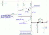
I've attached a schem, though it's a very standard configuration so should be familiar.
Cheers,
Attachments
Member
Joined 2009
Paid Member
I'm a big fan of the CFP configuration - and as far as I know so is Lumba so he'll be pleased if you get this working.
My next DIY project (in progress) has CFP output so I'm also vested in this and although I've used CFP in the front end I've never used it in the output.
In order to oscillate the output power device needs power. Perhaps you can choke off the oscillations at that point - note my careful choice of phrase
Hi Lumba,
I think next time I'll be using mosfets for the outputs, but now I've started with the BJT CFP (and bought the silicon...) I'm determined to get it working. I also think I'll learn something in the process. I'm pretty confident that the transistors are genuine; at least, they came from a reputable source (Rapid | Distributors of electronic components, electrical products and educational supplies), the cases look right and the Hfe at various collector currents is as expected. Maybe I should also check the fT? I know fakes are a big problem with Sanken/Toshiba devices...
Unfortunately I'm away on business so can't do much practically until I get back next weekend.
Cheers,
Atomicplayboy,
to avoid a lot of headache and disappointment, I would go for the diamond buffer topology (BJT in class AB).
to avoid a lot of headache and disappointment, I would go for the diamond buffer topology (BJT in class AB).
Just make a visual check.Maybe I should also check the fT?
- Status
- This old topic is closed. If you want to reopen this topic, contact a moderator using the "Report Post" button.
- Home
- Amplifiers
- Solid State
- Stabilizing CPF output stages