Hello,
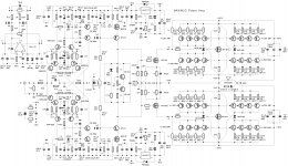
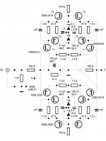
A complicated diagram that will be very difficult to put into practice. Imagine that you have to balance very well on the differential input stage voltage amplifier. With so many transistors in that stage, is very difficult but not impossible.
Your amplifier diagram will be a regrettable adventure DIY audio.
Let us know if succeeded or works this audio amplifier!!!
Best regards

My respects if you will face this monster...heheheheh.... exagerated!
be happy... as courage you already have.
Carlos
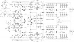
This monster, as you called it, I already faced splited in two different amps. Exactly the same VAS stage I employed in my StereoLith amp which has different output stage and exactly the same output stage I employed in my ProJet Power Amp module. So I said to myself why not to combine these two excellent parts in my next Maximus Power amp project.
So be it.
I will gladly take a role of a knight to face a "monster" amp and beat it.

Last edited:

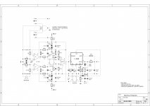
Maybe something similar to start working on in near future. Expert criticism wellcome.
Well, that's certainly ambitious.

Yes it is, but you probably don't know that I'm listening my StereoLith amp for a quite some years now and it is still simply the best sounding amp I had in my home.
After building StereoLith I said I'll never go to built such demanding and time consuming machine again, but as always, never say never again ... so it came that this year brought me a new pair of big speakers and I tried very hard to move some heavy amps to my home (Burmester 911, Esoteric A-03, Plinius SA110 ...) and still my homemade amp was simply better, more musical.
As you see now my only choice is to go further on from my verified past stages and do something, maybe even better.
Member
Joined 2009
Paid Member
Well it may look frightening at first, it's a big schematic, but the concepts inside it are all familiar. Seeing as you have proven out the building blocks already, seems that it has a chance. How on earth you optimize it though, lots of variables and pcb layout is a project all of itself. Looks as complicated as some commercial designs I've seen published around here.
I bet Digikey is looking forward to this too
I bet Digikey is looking forward to this too
...I will gladly take a role of a knight to face a "monster" amp and beat it.
Go Lakner, go !!!


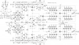
Schematic update: some minor corrections of tags, voltages and resistor power ratings.
That's the spirit juma.
That's a big amp Lazy Cat, it also looks like it should be extremely linear.
The OP stage looks a bit like the Bryston 28B
But I think the IP stage is probably nicer.
A question: why have you bypassed the IP stage 1k5 CFP BJT base R's with
1 uF? This will negate those 'helper' transistors above 100Hz or so, yes?
Keep us posted on the progress.
cheers
Terry
I agree that the value of 1uF cap should be smaller but without it you get really wild instability-oscillations as T2 interacts as current stabilizer to T1.
The whole idea of "combined" T1-T3 transistor instead of only T1 is junction thermal stabilisation of T1 (constant power dissipation) also well known as "memory distortion" elimination. At this T1-T3 combination, T1 has almost constant CE voltage provided by T3 and almost constant collector current provided by T2, so constan power is assured. When T2 is added to the circuit, current is divided between T1 and T2 and stability comes to be an issue. Adding 1uF cap stabilize conditions and I agree completely that its value should be optimized.
Maybe you have some better idea how to implement thermal stabilisation to T1, so please bring it out. My only wish is to still use SSM2210/2220 dual matched transistors in differential input stage.
Attachments
Last edited:
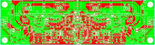
Maximus schematics configured as monoblock amp is as currently shown, divided in three major parts: VA stage populated on double sided PCB, positive combined BIGBT transistor on separate heatsink and negative combined BIGBT transistor on separate heatsink, hardwired with proper silver-plated Cu wire.
Combined power BIGBT (associated from 17 transistors) on heatsink will have only three connection points: 100 V, OUT and G, which is a good wireing practice when amp comes to assembly phase.
Also CFP BJT base 1 uF caps are being lowered to 1 nF which is adequate to impedance app. 1,5 k at 100 kHz and therefore determinate -6 dB point for the T2 parralel current transistor.
Current version attached:
Attachments
I see a lot of curiosity out there but no remarks.
No problem, just look and see if something from my schematics is appliable, some part, building block, that you can use in yours projects.
As you could find out yet, I very much like big solid state amps, I think that they have something more to give us, to enjoy musical experience deeply, thrillingly natural. So take an opportunity and once in a lifetime afford yourself a big, powerful amp.
Yes, many good features comes from cascoding and in Maximus input stage that was also the only possible solution to use SSM2210/2220 low CE voltage matched pairs. As seen 65 V supply potential is evenly distributed to cascoded trannies.
Also a step forward to more musical amp is constant power dissipation principle to differential input pair and mosfet gain transistor implementation in second stage, which is also cascoded for better performance.
Also a step forward to more musical amp is constant power dissipation principle to differential input pair and mosfet gain transistor implementation in second stage, which is also cascoded for better performance.
I was wondering if you are inspired by the memory distortion theories. I guess you are. If I get around to build a discrete amp again I will go for a low memory distortion design, but less complex and smaller than yours.Also a step forward to more musical amp is constant power dissipation principle to differential input pair and mosfet gain transistor implementation in second stage, which is also cascoded for better performance.
Why do you use MOSFETs as VAS?
Thanks for reply and you observation. To my opinion VAS is the most important part of amp regarding musicality and sound attributes in general, so it took me a lot of time in let say, last ten years to test all kind of combinations around symetrical VAS and especially local transistor stages like diff-amp pair and second gain stage. All small changes were always listened in the system and more musical version passed to the next level. The diff-amp with constant power principle was far more enjoyable then the other variants.
For the second gain stage normally is used BJT, which has for the purpose it serves, to small input impedance, drains quite some uA of current, which is unacceptable in a sense not to load collector resistance at all. So the first stage is immediately degraded with influence of the second one, but it should not feel it at all. In the way to relax first stage, constructors usually place a current mirrors instead of collector resistors but this ruin the musicality even worse. My idea for the gain transistor was to choose one without need to drain current and has small input capacitance and to be voltage driven, so the mosfet was the only logical choice. Of course it must be cascoded and implemented carefully regarding supply potential and loading current. But listening tests proved me right: it blew away all kind of BJT's like mist and sings music in natural, relaxed way, simply the best.
For the second gain stage normally is used BJT, which has for the purpose it serves, to small input impedance, drains quite some uA of current, which is unacceptable in a sense not to load collector resistance at all. So the first stage is immediately degraded with influence of the second one, but it should not feel it at all. In the way to relax first stage, constructors usually place a current mirrors instead of collector resistors but this ruin the musicality even worse. My idea for the gain transistor was to choose one without need to drain current and has small input capacitance and to be voltage driven, so the mosfet was the only logical choice. Of course it must be cascoded and implemented carefully regarding supply potential and loading current. But listening tests proved me right: it blew away all kind of BJT's like mist and sings music in natural, relaxed way, simply the best.
- Status
- This old topic is closed. If you want to reopen this topic, contact a moderator using the "Report Post" button.
- Home
- Amplifiers
- Solid State
- "Maximus Power Amp"