rbroer said:Any pitfalls and hints and suggestions ?
No I cant see any pitfalls.
A perfect circuit!
")
You can bet your last dime, if was anything to criticize
you would have had your share - and more ....
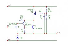
rbroer said:I've been looking into some buffers like Borbely and others and tried to add some ideas together.
Output DC offset will be handled upstream of the fet input
The input fet now operates constant power.
Any pitfalls and hints and suggestions ?
Is this for driving loudspeakers or something?
se
lineup said:possibly a subwoofer
Hehehe. Well just seems to be an awful lot of um... stuff just to drive a few feet of wire and a high impedance input.
se
Hi rbroer,
I trust the input FET is going to be gate biassed from somewhere?
Also I think you're biassing T4 from the +18V rail, wouldn't it be a good idea for C1 to bypass to that?
Seems to me unnecessarily convoluted for a simple need. please define your intent.
Cheers,
Greg
I trust the input FET is going to be gate biassed from somewhere?
Also I think you're biassing T4 from the +18V rail, wouldn't it be a good idea for C1 to bypass to that?
Seems to me unnecessarily convoluted for a simple need. please define your intent.
Cheers,
Greg
Re: Re: Cascoded jfet buffer
I found link to this very old thread (with 1900 views and no reply)
at Pedja Rogic gainclone page.
http://users.verat.net/~pedjarogic/audio/gainclone/gainclone.htm
He refers his solution to this thread
and also to a Nelson Pass paper:
Cascode Amp Design: by Nelson Pass
Steve Eddy said:Is this for driving loudspeakers or something?
se
amplifierguru said:Hi rbroer,
I trust the input FET is going to be gate biassed from somewhere?
Also I think you're biassing T4 from the +18V rail, wouldn't it be a good idea for C1 to bypass to that?
Seems to me unnecessarily convoluted for a simple need. please define your intent.
Cheers,
Greg
An externally hosted image should be here but it was not working when we last tested it.
I found link to this very old thread (with 1900 views and no reply)
at Pedja Rogic gainclone page.
http://users.verat.net/~pedjarogic/audio/gainclone/gainclone.htm
He refers his solution to this thread
and also to a Nelson Pass paper:
Cascode Amp Design: by Nelson Pass
Pedja Rogic
also recommends a more usual and simple alternative to buffer LM3875:
also recommends a more usual and simple alternative to buffer LM3875:
An externally hosted image should be here but it was not working when we last tested it.
amplifierguru said:Hi rbroer,
I trust the input FET is going to be gate biassed from somewhere?
Also I think you're biassing T4 from the +18V rail, wouldn't it be a good idea for C1 to bypass to that?
Seems to me unnecessarily convoluted for a simple need. please define your intent.
Cheers,
Greg
In the circuit in post 1:
The input FET should have some resistance to 0V reference or "ground" of the +/-18V supply, 1M to 10M is fine. No "ground" point is shown in the schematic, a glaring omission.
C1 provides low AC impedance from T4 gate to output, for current to drive T4 Cgd, just what you would want for a bootstrap cascode with highish Cgd. With 10mA sink current I would choose a JFET with high Idss and Vp instead of a power MOSFET, something like PN4391, connect R4 to output and dispense with C1,R6,R7. Yes there should be power supply bypass caps but in this schematic there is no 0V to connect to.
I have to wonder how stable the T1/T2/T3 compound feedback triple is. I've had enough trouble with oscillation in CFPs. Has anyone actually built this?
Post 1 is about 31 months old but rbroer has posted recently so a reply may come.
What is the value/purpose of C2? C1 will form a well defined pole with R1, but the C2 seems to form a pole with the rather variable ( part-to-part and temperature dependent ) transconductance of the input JFET.
The link in post 7 doesn't offer any clear explanation. I agree with this, but given 1/gm=33 ohms the -3db of C2 and 33 ohms is about 150kHz, well outside the audio range, so the variability might not matter. I would check for any signs of oscillation on the 2SK170 source.
Yes, this would be fine. I also have seen he is around.Post 1 is about 31 months old but rbroer has posted recently so a reply may come.
Regarding C2 in the gainclone circuit, I also find difficult to see the reason.
I dont know if Nelson Pass paper, PDF link above, on Cascoding will have something on this.
Joe Rasmussen does not use such a capacitor in his tube buffered gainclone, JLTi MK2.
http://www.customanalogue.com/
Joe Rasmussen does not use such a capacitor in his tube buffered gainclone, JLTi MK2.
Hmmm - looks like the BJT emitter voltage depends on the BJT base current, not a good design practice, better to add a resistor in parallel with the bootstrap capacitor. This voltage must be high enough for the plate but not too high so that the BJT saturates on positive peak input.
Steve Eddy said:
Hehehe. Well just seems to be an awful lot of um... stuff just to drive a few feet of wire and a high impedance input.
se
Hehe Hi Steve,
have you tried to compare driving a high impedance input from conventional medium Zout and from low Zout high current capability signal source?
Pavel
PMA said:have you tried to compare driving a high impedance input from conventional medium Zout and from low Zout high current capability signal source?
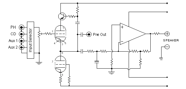
Why yes. Just take a look at my preamp.
An externally hosted image should be here but it was not working when we last tested it.
se
SY said:Don't laugh. There was at least one phono stage at ETF this year that was bigger than that.
Laugh? That's so sad it makes me want to cry.

se
Christer said:What's in that giant box Steve? A pot and a transformer?
Nah, just some pot.
Bong hits for everyone!
Hey, where's the bong hit smiley!? Oh, there it is.

se
Wow,
I might put my stereo Volume/FET cascode buffer which measures
2" x 1" x 1" -
http://www.diyaudio.com/forums/showthread.php?s=&threadid=70276
into a metre square block of machined rhodium with $$$ 4 zeroes price tag for Hi End street cred! Castors extra.
Cheers,
Greg
I might put my stereo Volume/FET cascode buffer which measures
2" x 1" x 1" -
http://www.diyaudio.com/forums/showthread.php?s=&threadid=70276
into a metre square block of machined rhodium with $$$ 4 zeroes price tag for Hi End street cred! Castors extra.
Cheers,
Greg
- Status
- This old topic is closed. If you want to reopen this topic, contact a moderator using the "Report Post" button.
- Home
- Amplifiers
- Solid State
- Cascoded jfet buffer