So no one has a reverse engineering on the SuperMos?
I built a SMOSII from scratch by bit stuffing a direct photoetch of a recovered board. It worked but never sounded right. I think a lot of the "Magic" of these amps lies in the matching of the output (and other) devices. Les said (from memory) the devices were custom built to his spec and he only selected the top 5% of production (more Les porkies or serious stuff!?!). It wasnt just about current sharing but overall linearity of the output stage. The devices were stated as being 250v 20A laterals which just didnt exist outside of Sage Audo. Even the dual die devices wernt around then (or were they
") ). It was one of the reasons given for why the SMOSII was so expensive.
). It was one of the reasons given for why the SMOSII was so expensive. Also the SMOSII was a very different beast from the superamp. The diagrams I (badly) drew out at the time were more complex than whats been put up so far. As mentioned elsewhere, the SMOS500 digram posted has 12 s/signal transistors, the board I built had 19.
De-pot and schematics of SuperMOS1
This is somewhere on the other thread too, but here's my SuperMOS1 de-pot and the schematic drawn up as a PDF:

SuperMOS1 Schematic (PDF)
This is somewhere on the other thread too, but here's my SuperMOS1 de-pot and the schematic drawn up as a PDF:
SuperMOS1 Schematic (PDF)


 The plot thickens.
 Brian sorry but I dont think that schematic will work.
Attached is the circuit I worked with to get simulations and it makes sense to me. I obtained them from the other thread. I think this is the suprmos2 circuit.
TripleJ, on the schematic I do count 19 transistors on the smos500. The use of TO220 parts in the smos500 cannot be used to account for the amount or lack of components, all components could have well been to92 s except for the output transistors.
ZeroD, judging by the other thread I think you have some information which might account for the difference in measured performance. Tell more about the small inductors, are these anywhere near the input transistors. This could account a little for the THD figures.
BTW is anyone interested in a build ??? Maybe we could get someone design a PCB.
Attachments
Last edited:
@ triplej
The output devices & some small signal transistors, whilst i knew Les, where hand matched & selected @ his place, by him. I personally hand matched & selected for him, numerous small signal transistors for hfe. He said all this made a significant difference to the specs/performance.
@ homemodder
The inductor was a small printed one etched out on the copper PCB track. I can't remember where exactly though. Here's an example of what it looked like. It's not exact, & the size was smallerr, but i hope you get the idea
Attachments

Yes, sorry, I just posted the "working it out" picture for a bit of a laugh! It does show the very simple single-sided PCB though, with no chance of any special PCB inductors on this design for sure (SuperMos-I).ahhhh... the pdf file is a real schematic!
Very possibly! But I did trace everything out very carefully, kept lots and lots of pictures, and double-checked everything, so it's really very close. The trouble is that one single error/connection can make a schematic look crazy, of course. I've really not looked at the circuit at all - I just drew it, and got distracted with other things... SuperMOS-II was quite different (as were other versions by what people say), but mine is what it is (roughly)! There's absolutely no doubt as to the number/type of transistors, resistor values etc. They all had their original markings and were easy to read during the de-potting process. The only exception was the o/p FETs, which had had their markings sanded off by the look of it.
Brian sorry but I dont think that schematic will work.
If you think there's a particular bit of the circuit that's obviously wrong, I might be able to revisit my notes and correct it (possibly!).
I'm sure that the matching process was important, which kind of makes building any more rather difficult, as do the unknown(?) o/p FETs. I very very much doubt they really were specially made for Les, but they might be unusual, and definitely matched.
All good fun, this
Thanks for the "working it out" picture of the de-potted SuperMOS1 and for the schematic. The picture brings back memories of my attempts to get inside my Superamp module. I didn't get very far because it is a lot of work and takes skill. I am impressed with your results.
I'm not convinced that the SuperMOS 500 will be stable in real life because my crude calculations show about 40 dB of gain at 20 kHz. I would like to see some simulation results such as a Bode plot or ideally a family curves at different operating levels.
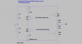
I think that the bias circuit relies on HFE ratio matching that's why selection was necessary. I have attached a picture showing my interpretation of it.
I'm not convinced that the SuperMOS 500 will be stable in real life because my crude calculations show about 40 dB of gain at 20 kHz. I would like to see some simulation results such as a Bode plot or ideally a family curves at different operating levels.
I think that the bias circuit relies on HFE ratio matching that's why selection was necessary. I have attached a picture showing my interpretation of it.
Attachments
I'm sorry I didn't really explain my thinking. No I don't think that the Vbe of Q15 and Q16 is setting the bias. I think that the bias is set by a current source and some transistor current gains hence the requirement for measuring and matching components with RV2 allowing a minor trim.
I am referring to the SAGE SUPERMOS 500 schematic. My explanation is that the current source formed by Q13 and Q14 shown as I1 in my diagram (I could have labelled it better) sets the current through Q15 and Q16 to about 10 mA.
R24 and R25 and the preset RV2 have quite a high resistance so have less effect and I omitted them from my simplified circuit.
The base current of Q15 (labelled Pre_driver_base_pos) and the base current of Q16 (labelled Pre_driver_base_neg) are then defined by their collector currents, collector to emitter voltages and temperature and should be relatively stable.
The base current of Q21 is defined so it's current gain sets it's collector current. Q20 is similar.
Any imbalance in base currents between Q21 and Q22 is corrected by the overall amplifier DC feedback loop.
The output MOSFETs Q22 to Q27 bias then depends on the voltage drops across R32 and R33 caused by the bias currents through Q21 and Q22.
I don't understand how the 'Active Class A' is supposed to work though.
Alternative explanations and / or simulations are welcome.
Hi Guys,
Re comment regarding FETs, it could well be that Les had parts selected for him, as SemiLab/SemiFab made or make the Hitachi clones for a number of HiFi companies and were not adverse to a bit of tweaking / customisation. The fact the part number had been removed is possibly a clue! Also the dual die plastic parts were notorious for local oscillation. This might be the source of the observed instability/RFI mentioned in this thread.
Glad to see the SuperMOS/Les sage thread is alive and kicking. We owe Les that much!
Thanks all for responding to the rejuvinated thread! I feel the bug biting again
Homemodder: For clarifaction: 19 TO92's, 7 TO220's and 6 (dual die) MOSFETS. Quite the beast!
TripleJ, on the schematic I do count 19 transistors on the smos500. The use of TO220 parts in the smos500 cannot be used to account for the amount or lack of components, all components could have well been to92 s except for the output transistors.
Homemodder: For clarifaction: 19 TO92's, 7 TO220's and 6 (dual die) MOSFETS. Quite the beast!
Thanks all for responding to the rejuvinated thread! I feel the bug biting again
Homemodder: For clarifaction: 19 TO92's, 7 TO220's and 6 (dual die) MOSFETS. Quite the beast!
scratch: The plot thickens even more. Exactly how many versions were there of this amp ???
Which version was this one, I could account for another 4 extra parts used that would improve performance and probably used by Les. I dont know what qualifications he had but he certainly was not a beginner.
As the time passes Im getting more determined to discover the circuits.Extra INFO etc
For those that aren't aware, a number of components were soldered together off the PCB, & then certain of those leads/legs soldered to the PCB. I saw these with my own eyes ! I asked him why, thinking they must have been afterthoughts/modifications etc, but he said that as there wasn't much room left on the PCB, & it all had to fit in the space allowed, so that was the only option. Apart from a larger PCB & potting box, which wouldn't have fitted in those heatsink cavities. Plus it didn't make any difference to the performance/specs, he added. This was on a 100W Amp, whether it was the Bipolar or Mosfet, i can't remember.
@ audiopip
Hi, great to see you're still interested, & posting Did you get round to doing those sims/builds you mentioned ?
For those that aren't aware, a number of components were soldered together off the PCB, & then certain of those leads/legs soldered to the PCB. I saw these with my own eyes ! I asked him why, thinking they must have been afterthoughts/modifications etc, but he said that as there wasn't much room left on the PCB, & it all had to fit in the space allowed, so that was the only option. Apart from a larger PCB & potting box, which wouldn't have fitted in those heatsink cavities. Plus it didn't make any difference to the performance/specs, he added. This was on a 100W Amp, whether it was the Bipolar or Mosfet, i can't remember.
@ audiopip
Hi, great to see you're still interested, & posting
Did you get round to doing those sims/builds you mentioned ?Bear you design yourself, what do you think of the schematics of posts 43 and 45.
Truthfully, I am a hack designer. Not a EE. Many on here are FAR more accomplished than I am! There is at least one 16yo I know of who is scary good... self taught too. I am an idiot by comparison. Heh.
Anyhow I scratched my head on what I have seen so far.
I think maybe these schematics are missing something here or there.
And I only took a very fast one time look, without any real thought at each of them so far.
It might be good to go out and ask some of the best designers on here like maybe EVUL and others to have a look. They can probably pick up on the details and what is wrong instantly, since they are fluent in terms of engineering. When I do circuit design, I need a stack of reference books around, and a simulator, plus occasional help from others... DOH!
If no one gets to it before i can I will try to stare at the schematic for a longer period of time and see if I can make it sink in. I am still trying to wrap my head around the "Allison" output stage. This one may be related, not sure, will have to compare and look at the connections and see what the "action" is... as I said, I'm slow and most of my knowledge is deeply embedded somewhere in mud within my brain.
It might be good to dump the schematics into a simulator and see what they are doing, should be easy to see any dynamic bias action then. Or lack thereof.
(anyhow, and talking to myself, doesn't dynamic sliding bias decrease the bias levels with increasing output swing? Not the other way around... so the max output power increases? Never really understood what the point of it is, because if you have enough heatsink to support a high class A quiescent current, then why bother shifting the amp into AB? I dunno... see? Otoh, you can keep the outputs from switching by moving the bias up with the signal... but then the speed of the bias circuit becomes an issue...)
But these clearly do not have enough heatsink for quiescent class A operation. No way.
Btw, I think I saw the ads for these modules in the back of Studio Sound mag, that came overseas from England to me back in the 70s...? Could be.
_-_-bear
----- dont men enything bad here but the two of you designed a 1KW amplifier that is perfect from every aspect ????? well i am very glad to inform you that mister Behringer has a team of engineers ( 20 ) to design his amplifier ....then another team of engineers to design the power supply for this amp ....and then another team of engineers to design the box for this amp and then another team to optimise the design cost wise ....and then another team to make it easy to use .....
Does it take that many engineers to operate a Xerox machine?
- Status
- This old topic is closed. If you want to reopen this topic, contact a moderator using the "Report Post" button.
- Home
- Amplifiers
- Solid State
- Les - Sage Audio - New Revelations