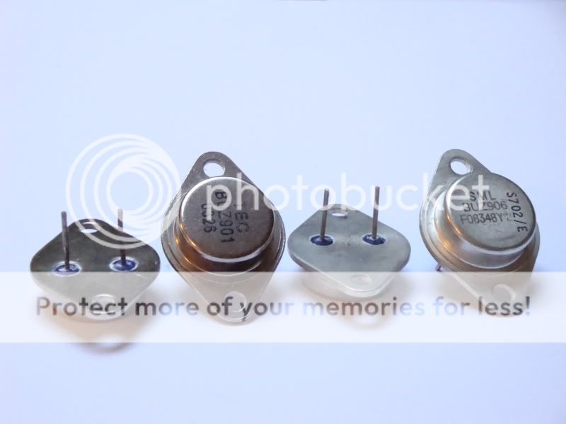
Found them in my local store, tested for Vgs at 30VDC and 30mA bias. Results are:
BUZ901
Vgs 615mV x 1 psc
Vgs 617mV x 3 psc
Vgs 618mV x 4 pcs
BUZ906
Vgs 847mV x 1 pcs
Vgs 866mV x 1 psc
Vgs 867mV x 1 psc
Vgs 869mV x 1 pcs
Vgs 875mV x 1 psc
Vgs 884mV x 1 psc
Vgs 890mV x 1 psc
Vgs 898mV x 1 pcs
Is there any other test I should do to see if they are real lateral M-fets or not?
BUZ901
Vgs 615mV x 1 psc
Vgs 617mV x 3 psc
Vgs 618mV x 4 pcs
BUZ906
Vgs 847mV x 1 pcs
Vgs 866mV x 1 psc
Vgs 867mV x 1 psc
Vgs 869mV x 1 pcs
Vgs 875mV x 1 psc
Vgs 884mV x 1 psc
Vgs 890mV x 1 psc
Vgs 898mV x 1 pcs
Is there any other test I should do to see if they are real lateral M-fets or not?
hi
i agree with jaycee the TEC ones look suspicious, i understood that Magnatec were a brand name of SEMELAB as is SML.
see here http://www.semelab.com/magnatec/mosdata.shtml
an email to the guy at foot of the page should clear up the confusion
i agree with jaycee the TEC ones look suspicious, i understood that Magnatec were a brand name of SEMELAB as is SML.
see here http://www.semelab.com/magnatec/mosdata.shtml
an email to the guy at foot of the page should clear up the confusion
Thanks all for replay
Could you elaborate how to do it?
Also, found this http://www.bilder-hochladen.net/files/1kxe-73.pdf
On line translation from german to english:
"BUZ901 Here first times the mentioned transistor And here the left to the data sheet http://www.magnatec-uk.com/pdf/magnatec/BUZ900.pdf On the fast one we can take the data sheet the following! We go again to my copy: After data sheet it would have to be so occupied. Thus as next would like I unite measurement with the component tester of my oscilloscope to present. First measurement: on the gate, otherwise this measurement a short-circuit can pretend the connections of the component tester between SOURCE and drain, a finger, if a remainder load at the high impedance gate connection is present. To mark I would like still that it a N-type concerns. To the component tester: In X-direction the tension in Y-direction the river. On that right side will the red connection positive, to the left of the 0-Linie (centric) becomes negative it. The sharp break on the right side shows upward that the transistor is leading reverse. On the left side the triangle form forms, by my contact with the finger. A cause is for it the frequency ☺ That is a typical behavior for an enhancement-mode. But stop, why it becomes on the positive page reverse leading. It acts nevertheless around a N-type. SOURCE is appropriate for gate Drain SOURCE but at mass of my component tester, normally thus the sharp break would have up go to the left side downward, and on the right of the gate influence become evident. We go to the thing on the reason: In the next attempt I short circuit now the gate with the SOURCE connection. SOURCE is after data sheet the housing. Now however the behavior does not fit absolutely any longer! Normally the transistor would be allowed to do only the break up-white, where it becomes leading reverse. Only explanation: The housing is that drain and not SOURCE. We continue to go out however of a N-type. Now I want to know it and wedge times the short circuiting bridge between the two pins: Now however the transistor closes as it belonged and shows up only the break for „the Rückwärtsbetrieb “thus must that SOURCE, pin two be, now is also clear it, why the break is on the wrong side. Thus we put the black ones to repeat now at pin 2 and the red one to the housing and the measurements: Now the assumption is set up: Pin 1 gate Pin 2 SOURCE Housing drain N-type Short circuiting bridge between gate and SOURCE, red at the housing: First point for the assumption! Short circuiting bridge between gate and drain, red at the housing: Second point for the assumption! Something alternating voltage over the finger at the gate, red still at the housing: The third point! Everything points nevertheless now on it: 1=Gate, 2=Source and Case are drain, or not?"
jaycee said:Do the acetone test on the cases.
Could you elaborate how to do it?
Also, found this http://www.bilder-hochladen.net/files/1kxe-73.pdf
On line translation from german to english:
"BUZ901 Here first times the mentioned transistor And here the left to the data sheet http://www.magnatec-uk.com/pdf/magnatec/BUZ900.pdf On the fast one we can take the data sheet the following! We go again to my copy: After data sheet it would have to be so occupied. Thus as next would like I unite measurement with the component tester of my oscilloscope to present. First measurement: on the gate, otherwise this measurement a short-circuit can pretend the connections of the component tester between SOURCE and drain, a finger, if a remainder load at the high impedance gate connection is present. To mark I would like still that it a N-type concerns. To the component tester: In X-direction the tension in Y-direction the river. On that right side will the red connection positive, to the left of the 0-Linie (centric) becomes negative it. The sharp break on the right side shows upward that the transistor is leading reverse. On the left side the triangle form forms, by my contact with the finger. A cause is for it the frequency ☺ That is a typical behavior for an enhancement-mode. But stop, why it becomes on the positive page reverse leading. It acts nevertheless around a N-type. SOURCE is appropriate for gate Drain SOURCE but at mass of my component tester, normally thus the sharp break would have up go to the left side downward, and on the right of the gate influence become evident. We go to the thing on the reason: In the next attempt I short circuit now the gate with the SOURCE connection. SOURCE is after data sheet the housing. Now however the behavior does not fit absolutely any longer! Normally the transistor would be allowed to do only the break up-white, where it becomes leading reverse. Only explanation: The housing is that drain and not SOURCE. We continue to go out however of a N-type. Now I want to know it and wedge times the short circuiting bridge between the two pins: Now however the transistor closes as it belonged and shows up only the break for „the Rückwärtsbetrieb “thus must that SOURCE, pin two be, now is also clear it, why the break is on the wrong side. Thus we put the black ones to repeat now at pin 2 and the red one to the housing and the measurements: Now the assumption is set up: Pin 1 gate Pin 2 SOURCE Housing drain N-type Short circuiting bridge between gate and SOURCE, red at the housing: First point for the assumption! Short circuiting bridge between gate and drain, red at the housing: Second point for the assumption! Something alternating voltage over the finger at the gate, red still at the housing: The third point! Everything points nevertheless now on it: 1=Gate, 2=Source and Case are drain, or not?"
The Vgs voltages seem very high for Laterals passing 30mA.
I get around 500mV for 100mA with 1058/162 when matching them
I get around 500mV for 100mA with 1058/162 when matching them
That's my opinion as well, as Vgs at original 2SK134/2SJ49 in an Sanyo Plus P55 power amp, according to service manual, should be at ~400mV with +/-58,5VDC supply and 25mA of bias. So, it seems they are fake, right?
aparatusonitus,
not necessarily, just different from the Hitachi devices. I still would use them.
not necessarily, just different from the Hitachi devices. I still would use them.
Lumba Ogir said:aparatusonitus,
not necessarily, just different from the Hitachi devices. I still would use them.
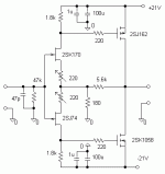
So, you are suggesting to try them in an real circuit...maybe like this regs from Kaneda ('cos I only have +30V/2A variable regulator at my disposal right now)?
http://www.diyaudio.com/forums/attachment.php?s=&postid=508975&stamp=1100036521
Lumba Ogir said:I still would use them.
Of course. The devices look like pulls. If they came from a surplus outlet or otherwise secondhand with residual white thermal grease it's a sign that they came out of something that was in all likelihood, working. If they were fakes they would have blown up in the original application.
As long as there is no physical damage, i.e., cracked seals, I have no problem using pulls. It is sometimes the best way to get rare or out of production devices.
wg_ski said:The devices look like pulls.
No, they are brand new ones, thermal grease is aplied by me while testing.
aparatusonitus,
I would definitely use them in a power amplifier, even if they cannot compare with the devices manufactured by Hitachi. Please consider the design in post #7.
I would definitely use them in a power amplifier, even if they cannot compare with the devices manufactured by Hitachi. Please consider the design in post #7.
Figured out what is "acetone test" and I can tell that SML BUZ906 passed this test, but that is not the case with the TEC BUZ901.
aparatusonitus said:Is there any other test I should do to see if they are real lateral M-fets or not?
If pinout is with case = source they are lateral. If case = drain they are some kind of vertical device. It could be cheated by not attaching the chip to the case, but in that case it would be very fake indeed and fail at 500mW or so of power dissipation

The SML branded ones are made by Semelab and appear genuine.
The ones branded TEC might well be Magnatec but they look a bit suspicious. Do the acetone test on the cases.
about the URL
aufzu Halbleiterhersteller-Logos-Ecke
you will find a wide range of logos. But I don't find there the logo "TEC" and also not the Magnatec-logo from the attachement.
I will ask by Magnatec what about the logo "TEC" on the transistor without the rest from the attachement.
Attachments

Last edited:
- Status
- Not open for further replies.
- Home
- Amplifiers
- Solid State
- Genuine BUZ901/906 or not?