Hey everyone,
I am building a smaller amp with maybe 20 watts per channel. I am routing all of the power traces for 50 mils and the traces I do not expect much power on for 25 mils. Is this a good assumption? I was thinking about going with 75 mils for power. Is this overkill?
Also, I have decided to go with a double sided pcb since I have like 80 parts to route. Basically, the traces I could not fit all on one side I put on the other. Is it ok to do this? Will it cause noise? I have heard some people say to put all power and ground on one side and everything else on the other. Any rule of thumb for this?
Thanks,
Mark
Generally speaking, yes - the power and ground traces are usually on the bottom of a two-sided PCB - all of your signal traces are on the top. This makes troubleshooting much easier (if you want to probe a certain signal, you don't have to flip the board upside down).
Just another suggestion for you - depending upon what kinds of components you are using (surface mount, lead-less packages, etc.), I would suggest that you do NOT get a solder mask on your board. This way, if your traces are too thin, then you can solder some bus wire right over the top of them to enhance their current carrying capability. If you have a solder mask, you would have to scrape the solder mask away from your traces before doing this.
Do a google search for
pcb trace width calculator
This should get you to several pages that can give you numbers as to how thick a PCB trace should be for a given current.
One inch of 50mils 1 oz thick copper has a DC resistance of about 11 milliohm. A 20W amp into 8ohm will have a peak current of 2.2A, hence a voltage drop on critical traces of max 24mV peak per inch. That's way to much to my taste, I would double the high current traces width. Even so, you would still require a good layout to avoid ground loops.
syn08 said:One inch of 50mils 1 oz thick copper has a DC resistance of about 11 milliohm. A 20W amp into 8ohm will have a peak current of 2.2A, hence a voltage drop on critical traces of max 24mV peak per inch. That's way to much to my taste, I would double the high current traces width. Even so, you would still require a good layout to avoid ground loops.
I agree with this. Another option is to go with 2 oz copper (or heavier) also. This will make very little difference in price for small runs of just a few pieces.
If you have room, you can go with both our suggestions.
If your PCB CAD software allows powerplanes I would use them as much as possible to keep the ground plane as low impedance as possible.
Otherwise fill out tracks the best you can.
I would use a minimum of 75 thou and thicken up where room allows.
I have a 900w amp and use upto 200 thou tracks on high power lines.
Otherwise fill out tracks the best you can.
I would use a minimum of 75 thou and thicken up where room allows.
I have a 900w amp and use upto 200 thou tracks on high power lines.
An externally hosted image should be here but it was not working when we last tested it.
See if you can use 100 mils for most of the power and output nodes. Where this isn't workable you can narrow the trace -- I'm lucky to be able to "right-click" to narrow or widen the trace, but ymmv.
When you discover a mistake with a solder mask, just grab the Dremel with a cutting blade.
Audioman45 suggested (in an Application Note) that groundplanes weren't helpful in audio amp circuitry -- so I laid out another board using the LM4702 sans ground plane, using a central locus to bring the signal ground together. The difference was measurable in terms of the THD% being a smidge lower, and by a smidge I mean a tiny but consistently measurable amount.
I dont know
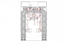
This one has supply caps all the way from bridge to output
Maybe thats slightly different
Oh, connections from power transistors to speaker out will be solid core wire
Well, the whole thing might be hard wired, or just part of it
I should say this too, its a Dx amp
This one has supply caps all the way from bridge to output
Maybe thats slightly different
Oh, connections from power transistors to speaker out will be solid core wire
Well, the whole thing might be hard wired, or just part of it
I should say this too, its a Dx amp
Attachments
Indeed, you want the two rails as close together as possible, to minimize loop area. However, it is a lot easier to lay out a PCB with one rail on each edge.Eva said:Visually symmetric layouts with rails on the sides and small signal stuff in the middle are the worst.
Mr Evil said:
Indeed, you want the two rails as close together as possible, to minimize loop area. However, it is a lot easier to lay out a PCB with one rail on each edge.
That example posted isn’t any good but a rail on each side can be perfectly fine - it's where the power leads terminate and where the current flows that counts. And "visual symmetry" isn't and evil either. There are a number of designs around with both symmetry and rather large “loop areas” (due to mechanical constraints) that still achieve very low distortion.
Also, laying out a class B or AB power output stage with the power supply rails overlayed is often misguided because the field of one half wave will not cancel that of the other.
Same goes for twisting supply rail wires together without the ground return.
from ....a post from user
Eva ....
the ideal pcb will have a small power and ground traces ( lengthwise ) and have this type of stracture :
from left to right ...totally left side the power things outs drivers vbe multiplier ..... in the center ,ground may be power caps ( if no more than 4) and on the totally oposite side right area the small stuff like LTP ccs VAS and goes on ...
ground plane can always be tricky
destroyes your star ground pholosofy
can create capacitance between the other layer
On a very related subject, once I create a PCB layout, using some appropriate software, currently tinkering with diptrace, how do I go about gettting a PCB created? Is there a service in the UK (actually I do not care where in the world) that would create a PCB for me (even undrilled) ?
Eva said:Visually symmetric layouts with rails on the sides and small signal stuff in the middle are the worst.
G.Kleinschmidt said:
That example posted isn’t any good but a rail on each side can be perfectly fine
Yeah, thats what I have been told numerous times in relation with another design, but it works ok though, as Glen says
Though I wonder if the ground loop issues might be different, when common ground is placed at the end of power supply, close to output stage
Thanks
")
Mr Evil said:
Indeed, you want the two rails as close together as possible, to minimize loop area.
However, it is a lot easier to lay out a PCB with one rail on each edge.
That was the point
That the benefits from having supply lines and ground plane end right at the output stage holds enough benefits to override the other issues on hand
And there ought to be some benefits from having no supply wires at all, other than trafo connections
Compromises there will be anyway
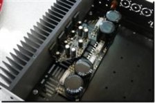
Below is from Holton site
Could be an option, but seems to me like there might be other issues with bridge so close to amp curcuit
Additional noise from wire connections etc
Probably works fine though
Attachments
akis said:On a very related subject, once I create a PCB layout, using some appropriate software, currently tinkering with diptrace, how do I go about gettting a PCB created? Is there a service in the UK (actually I do not care where in the world) that would create a PCB for me (even undrilled) ?
Hi,
I've had good luck with pcbfabexpress.com and custompcb.com.You just send them your gerbers by the web. A lot of people have used olimex with good results - their shipping costs are a little high to the US. Any of these companies will drill them for you so don't worry about that.
If you want to try making your own try http://www.fullnet.com/~tomg/gooteepc.htm where there is an explanation of how to make pcb's using a laser printer. It works quite well for one sided boards. Haven't tried double sided boards yet.
Charlie
On a very related subject, once I create a PCB layout, using some appropriate software, currently tinkering with diptrace, how do I go about gettting a PCB created? Is there a service in the UK (actually I do not care where in the world) that would create a PCB for me (even undrilled) ?
[/UnQuote]
Send your gerber files to this bloke.
I have had excellent PCB's back at good prices.
lorimer888@tiscali.co.uk
- Status
- This old topic is closed. If you want to reopen this topic, contact a moderator using the "Report Post" button.
- Home
- Amplifiers
- Solid State
- PCB Trace widths