After many E-mails and even a few download attempts at my "supersym" PCB ( It's not done yet.. have patience  )
)
, I am starting a new thread to : 1. Share the existing amp (PCB and construction advice) , 2. Design a professional board that will maximize performance and fidelity. , and 3. develop it further with JFET inputs (anatech's suggestion)and a MOSFET OPS.
The design as it is now...
It has been the best sounding by far of my DIYA creations.
It stays biased within 2mv , any environment , drives paralleled 15" 3-ways all day at full volume .. no turn-on thump , completely stable in every way.
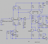
The base schematic is here ..
I am using C21 as my HF compensation. I have a 470K in place
of c6/r13.
Attached is the LT file to see for yourself (all models included). Make sure the "supersym .txt" in the zip file is in the same directory as the .asc file (models)..
OS
), I am starting a new thread to : 1. Share the existing amp (PCB and construction advice) , 2. Design a professional board that will maximize performance and fidelity. , and 3. develop it further with JFET inputs (anatech's suggestion)and a MOSFET OPS.
The design as it is now...
An externally hosted image should be here but it was not working when we last tested it.
It has been the best sounding by far of my DIYA creations.
It stays biased within 2mv , any environment , drives paralleled 15" 3-ways all day at full volume .. no turn-on thump , completely stable in every way.
The base schematic is here ..
An externally hosted image should be here but it was not working when we last tested it.
I am using C21 as my HF compensation. I have a 470K in place
of c6/r13.
Attached is the LT file to see for yourself (all models included). Make sure the "supersym .txt" in the zip file is in the same directory as the .asc file (models)..
OS
Attachments
This is a very good idea..forum needs something more modern
to avoid be running over the same old story again and again.
This is a lovely amplifier, with astounding dinamics and nice sonics, and has room to developments...not too much explored..only few guys made modifications on it.
Then you will be offering something good for us to assemble, and will be decreasing our forum "agging", as we were turning a lot of oldies doing only ancient designs.
All i could do was my old style schematics...but for sure you can do something more modern as you are younger than me and more modern inside your mind.
This one is much more modern, some folks said Sansui made into the eigthies..but i could never find that Sansui schematic that matches.
Maybe a Marantz had schematic almost alike.
I love this amplifier performance.... wonderfull gift Michael Bittner left for us.
regards,
Carlos
........................................................
Nobody has made the "forum" amplifier, with a selection of subcircuits... alike to use the most brilliant ideas...input from Roender, second stage from Symassym and output from other guy.... some forum different circuit, with all our good ideas united.
Member
Joined 2009
Paid Member
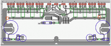
ostripper said:I have only gotten this far on the PCB , I whether a am wondering whether a 3 X 9" with opposed output pairs would be a better
design instead of "the long way" (Attached).
OS
Hi OS,
This looks interesting.
my 2c: the pcb shape and output device arragement might depend on how you feel this would be heatsinked ? Some people have chasis where it's convenient not to have the opposing pairs but like to put them all along one edge.
The other thing is whether you would have a benefit if you were to route the main power busses around the opposite sides of the board, this puts all the circuitry inside the 'magnetic flux loop' created by these high currents - can you route the heavy traces along one side only so that +/- are next to each other (most elegantly done with 2-sided pcb but TGM1 did it one side since it has a wimpy current compared with your beast) ?
By DX - to avoid be running over the same old story again and again.
I will be good here , Carlos..
 Even as this is similar to Mike B's design , it is NOT. It is running at 77v rails , has twice the bandwidth of the "sym" ,different CCS , and a "turbo" output stage.
When the board is done it will also have a cascode and jfet inputs , I
have actually built, designed and listened to a smaller version with these mods. At this point it really IS NOT a symasym any more. Something closer to it can be found here (Copyright).
http://ampslab.com/bi240.htm The original has not been "supersized" to this point, so this thread is to explore that aspect.
A real good observation.... I have tried this amp with just C7 , just C8 , stays stable-sound does not change. The only benefit of the 2 Cdoms is that they load the LTP equally at low levels.By forr - I wonder if C7 is really useful.
By BIGUN- The other thing is whether you would have a benefit if you were to route the main power busses around the opposite sides of the board, this puts all the circuitry inside the 'magnetic flux loop' created by these high currents - can you route the heavy traces along one side only so that +/- are next to each other (most elegantly done with 2-sided pcb but TGM1 did it one side since it has a wimpy current compared with your beast) ?
Yours is not "wimpy"
seriously , you have read my mind again, while laying out the 'opposing" pair layout (attached) , I noticed all the traces were running parallel , these were not at right angles and parasitics might "erupt". Not good for an amp like this.the board layout I already posted will fit on a 5" X 10/15" HS.
OS
Attachments
Make room for a cascode in the LTP - beneficial with both transistors and FETs in the front end. Use a triple output - IMO this is the best output stage type, every time I have looked at it, it reduces THD considerably.
Absolutely , a 30 volt zener biased cascode with the choice of Jfets or SMD dual matched lower Vce devices would perform very nicely.
The triple would only be needed with lower beta MJ's (TO-3) or more than 5 pairs. At 4 pair and 2R the VAS only sees .4ma load
(this is where the .002-3% extra THD comes from). that is very acceptable for a type 2 EF passing 15A (way above the SOA of these devices).
The triple , while I have worked the stability issue out , adds parts and complexity with such a small return.( .006 vs .01 @ 2R /15A/ 20k)
Try it on the spice file , add some mje340/50's or mpsa42/92's predrivers. 1K emitter resistance, 3.3k for the upper Vbe resistor. It works nearly the same.
OS
Member
Joined 2009
Paid Member
Originally posted by ostripper ... while laying out the 'opposing" pair layout (attached) , I noticed all the traces were running parallel , these were not at right angles and parasitics might "erupt". Not good for an amp like this.
We're talking the same words but about different things, I think...
I was asking if you wanted to purposely route the power rails adjacent and parallel to each other, a bit like how some folks twist together their power feed wires.
It puts the power rails on one side and allows you to put the sensitive signal wiring over on the other side of the pcb. That way large currents stay away from small currents with no big current loops (magnetic parasitics).
Well, just a thought
I do want to understand more about the Bass. People have commented that supersym has outstanding 'slam' compared with some other amps. Why ? It has to be more than having a 2.2uF input cap.
ostripper said:
The triple would only be needed with lower beta MJ's (TO-3) or more than 5 pairs. At 4 pair and 2R the VAS only sees .4ma load
(this is where the .002-3% extra THD comes from).
What is the current of his Vas?
in a real circuit they can get hot enough
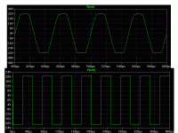
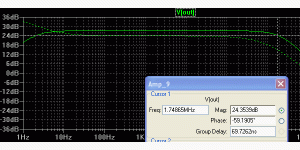
By raphael - Loop DC (without input filter) 1,7Mhz -3dB I will take problem?
You might have your LT probe on the wrong side of the NFB resistor.
I usually put (c) as output , (a) as the base of the feedback LTP transistor. Probe goes between (c) and the NFB resistor (27kj in this case.
Attached is plot of V(c) and -V(c) / (a).
OS
Attachments
ostripper said:
You might have your LT probe on the wrong side of the NFB resistor.
I usually put (c) as output , (a) as the base of the feedback LTP transistor. Probe goes between (c) and the NFB resistor (27kj in this case.
Attached is plot of V(c) and -V(c) / (a).
OS
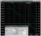
I put my closed loop, measured directly in the output.
Not understand what you are measuring? (open loop?)
Originally posted by ostripper
Try it on the spice file , add some mje340/50's or mpsa42/92's predrivers. 1K emitter resistance, 3.3k for the upper Vbe resistor. It works nearly the same.
OS
Try it with the KSA1381/KSC3503 as the predrivers
should be a lot of difference.I questioned the need for a triple on a low power amp like my Adastra, but when I tried it (using KSC1845/KSA992 for predrivers there) the drop in THD was significant enough to warrant me keeping them. I suppose the difference there is that that isn't a differential VAS.
Hi ostripper,
Try to keep the voltage across the input diff pair lower than 8 or 9 VDC if you can. A 6 V drop might be a good target. Allow the cascode transistors to soak up the excess.
I really, really dislike mosfet output stages. Jan made the only one I have liked the sound of so far, and that was an error correction amp.
One suggestion for you. Why not design it as a voltage amp PCB and an output PCB? That way you can keep the temperature changes around the voltage amp section minimal, and allow for nice, thick traces for your output transistors. A side benefit is that this would allow you to try out different output sections easily, same for voltage amps. Just a thought.
-Chris
Try to keep the voltage across the input diff pair lower than 8 or 9 VDC if you can. A 6 V drop might be a good target. Allow the cascode transistors to soak up the excess.
Please, BJT's?and a MOSFET OPS.
I really, really dislike mosfet output stages. Jan made the only one I have liked the sound of so far, and that was an error correction amp.
One suggestion for you. Why not design it as a voltage amp PCB and an output PCB? That way you can keep the temperature changes around the voltage amp section minimal, and allow for nice, thick traces for your output transistors. A side benefit is that this would allow you to try out different output sections easily, same for voltage amps. Just a thought.
-Chris
By bigun - I was asking if you wanted to purposely route the power rails adjacent and parallel to each other, a bit like how some folks twist together their power feed wires.
Let's get right to it ! First let's see how the pro amps do it...
First is a Yamaha 300w (pro amp).
An externally hosted image should be here but it was not working when we last tested it.
Here it looks typical with fat rail traces running parallel to the main emitter resistor rail (output)and the basestopper traces above that. any small signal stuff is away from this heavy current.
My scheme is similar to the yamaha rail wise. I noticed on all the OEM's the grounds go everywhere and only become "sane" at the main caps (a real star) , the OEM's even use off value caps to decouple (counteract) parasitics from long ground traces...

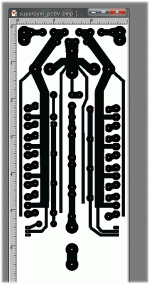
We can do better. On the rest of the board I "wrap" the Main caps ground return around the outside of the board with the lower level rail (VAS and LTP) ground returns inside of that. So anywhere at the back of the board is "surrounded" by the low current returns.Inside of those 2 groups of ground traces ,I then try to completely surround the LTP and input components with the "lifted" ground (R27 - 22r). All 4 of the capacitor ground returns are equal in length. See the image.
An externally hosted image should be here but it was not working when we last tested it.
Also since the amp is referenced off of that main "star" in the middle , the speaker return should go there to (ZERO hum).
JVC and others do the "Copper bar thing" emulating a double sided layout by soldering copper bars on the component side of
the PCB. It works ,I did this on the "little' supersym. (Gave them PCB's to Danielwritesback).
An externally hosted image should be here but it was not working when we last tested it.
The zobel ground and the NFB return also have an ideal setup. The zoble return should not snake through the input section or even the VAS , a straight wire back to the star is good. The nfb
should be attenuated by its resistor AT the takeoff point , then run through a shielded wire grounded to the signal ground at the LTP.
OS
Ahh , howdy.. Chris..
Hmm , at a proposed 70 volt rail , and the fact that mouser has a WIDE selection of 60V zeners, (seems to be a common popular value)http://www.vishay.com/docs/85588/1n5221b.pdf
I see why you said 9V , Jfets are becoming obsolete at 30v and above , so if i do it this could be the way ..
http://www.onsemi.com/pub_link/Collateral/NTUD3170NZ-D.PDF nice matched pair mosfet , back to back zeners , 20v VDss.. But you hate mosfets .
As far as OUTPUTS , quasi (power amp under development) has shown the IRF240 /9240 are very interchangeable with BJT's . His "brother of quasi" is a clone of his NMOS 350 , except for a different Vbe and gate protection. I can most likely predict that a
supersym with IRF's would sound nearly the same as with the BJT's but have double the SOA and be a 350 watt /8R- 500w /4R amp.
(Don't worry , NJW'S and the 2sc5200's are the main project.. you can't take away my BJT's)
What IS a problem is jfet and Mosfet LT models.. nowhere as good as the BJT's.
OS
by anatech - Try to keep the voltage across the input diff pair lower than 8 or 9 VDC if you can. A 6 V drop might be a good target. Allow the cascode transistors to soak up the excess.
Hmm , at a proposed 70 volt rail , and the fact that mouser has a WIDE selection of 60V zeners, (seems to be a common popular value)http://www.vishay.com/docs/85588/1n5221b.pdf
I see why you said 9V , Jfets are becoming obsolete at 30v and above , so if i do it this could be the way ..
http://www.onsemi.com/pub_link/Collateral/NTUD3170NZ-D.PDF nice matched pair mosfet , back to back zeners , 20v VDss.. But you hate mosfets
.As far as OUTPUTS , quasi (power amp under development) has shown the IRF240 /9240 are very interchangeable with BJT's . His "brother of quasi" is a clone of his NMOS 350 , except for a different Vbe and gate protection. I can most likely predict that a
supersym with IRF's would sound nearly the same as with the BJT's but have double the SOA and be a 350 watt /8R- 500w /4R amp.
(Don't worry , NJW'S and the 2sc5200's are the main project.. you can't take away my BJT's)
What IS a problem is jfet and Mosfet LT models.. nowhere as good as the BJT's.
OS
Hi Ostripper
---The only benefit of the 2 Cdoms is that they load the LTP equally at low levels.---
My concern is that current flows through C8 because of the varying voltage at Q5 collector, but Q6 collector voltage being almost fixed at about +0.6 V above ground, current variations in C7 can only be very small. So I don't think we can consider that C7 and C8 load the LTP collectors equally.
- Status
- This old topic is closed. If you want to reopen this topic, contact a moderator using the "Report Post" button.
- Home
- Amplifiers
- Solid State
- Symasym - the next generation (supersym)