Hello.
I haven't been on here for some time as I was tending to matters not electronically oriented. But it feels good to be back.
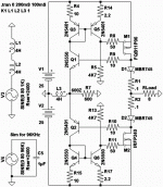
After the long break I came up with this. To me it seems more practical than my others. With my recent obsession over the Allison, I thought I would take a break from trying to improve it and make a circuit using the original idea.
It's still only in simulation. Time rolls by, but so far no money to do anything with. But one good thing: I have a broken Harman/Kardon AVR 35 sitting beside me waiting to either be fixed, or to be gutted, possibly for organ transplants with my new design. I think the only thing wrong with it is blown output devices but I need a service manual (anyone have one handy?") ).
).
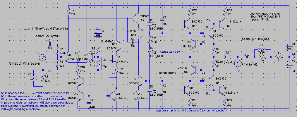
The VAS is cascoded, something which I noticed does nicely to reduce distortion. The FET CCS is cascoded to reduce PSRR (this was an experiment of mine, I was wondering if I could use fewer parts). All CCS's are cascoded, except in the output stage, as they are all important.
Squarewave is good, but the thing mangles anything above 50KHz, I think because of the Cdom value. C9 and C10 really help stability.
Because of the cascodes, it won't go rail-to-rail output, but I think that's just fine.
THD@40W, 1KHz = .00028%
THD@40W, 20KHz = .00059%
Note that these are simulated values, I cannot predict what will happen if it is built.
Simulation file is attached. If you need models, say so.
Thank you for your time and any comments or suggestions.
- keantoken
I haven't been on here for some time as I was tending to matters not electronically oriented. But it feels good to be back.
After the long break I came up with this. To me it seems more practical than my others. With my recent obsession over the Allison, I thought I would take a break from trying to improve it and make a circuit using the original idea.
It's still only in simulation. Time rolls by, but so far no money to do anything with. But one good thing: I have a broken Harman/Kardon AVR 35 sitting beside me waiting to either be fixed, or to be gutted, possibly for organ transplants with my new design. I think the only thing wrong with it is blown output devices but I need a service manual (anyone have one handy?
).The VAS is cascoded, something which I noticed does nicely to reduce distortion. The FET CCS is cascoded to reduce PSRR (this was an experiment of mine, I was wondering if I could use fewer parts). All CCS's are cascoded, except in the output stage, as they are all important.
Squarewave is good, but the thing mangles anything above 50KHz, I think because of the Cdom value. C9 and C10 really help stability.
Because of the cascodes, it won't go rail-to-rail output, but I think that's just fine.
THD@40W, 1KHz = .00028%
THD@40W, 20KHz = .00059%
Note that these are simulated values, I cannot predict what will happen if it is built.
Simulation file is attached. If you need models, say so.
Thank you for your time and any comments or suggestions.
- keantoken
Attachments
Do you mean RMS power or something? I still haven't gotten the RMS thing down yet. But the max output is 40V pk-pk. So +20V/8=2.5, 2.5*20=50W. Okay, I'll bet I'm doing this in a very nonstandard way.
Oh well. You probably get what I mean. Bias current is 1.5A. So maximum current is 3A, though to get this much out we would have to use a smaller load because the output swing is limited by the cascodes.
J2 has about 2.4V on it. Is this not optimal? I know nothing about Jfets.
- keantoken
Oh well. You probably get what I mean. Bias current is 1.5A. So maximum current is 3A, though to get this much out we would have to use a smaller load because the output swing is limited by the cascodes.
J2 has about 2.4V on it. Is this not optimal? I know nothing about Jfets.
- keantoken
keantoken said:Do you mean RMS power or something? I still haven't gotten the RMS thing down yet.
- keantoken
((20/sqr2)^2)/8 = 25W
Keantoken,
At about the same time that you posted your circuit here (midday my time), I was just printing out a similar design for a small Class A Allison bias amplifier. As your output stage was so similar to mine I thought I'd compare them - they weren't the same!
Your output stage has a nasty high frequency response peak around 1 MHz (I think) that would almost certainly cause it the real circuit to oscillate. It took some time to determine why my design didn't have this effect. The final solution was an emitter resistor in the output driver transistors, plus a more conventional Allison frequency compensation scheme - see attached pdf.
Some other minor things:
- LED current was too high,
- Allison bias current could be a bit higher,
- BC54x transistors are not suitabe as drivers, as the power dissipation is too high. Use mje340/350 or BD139/140 or similar.
- I haven't looked at the input stage.
Yesterday I did a large number of LTspice simulations comparing overalll feedback and no overall feedback. Some interesting results:
- Overall feedback reduced THD, by reducing 2nd and 3rd harmonics, but slightly increased the higher orders.
- Looking at the 7th harmonic (the really nasty one), overall feedback actually increased this distortion.
If I build one of these amplifiers, I'll use feedback around the input stage, and no overall feedback. While the THD is worse, the spectrum looks better! I'm currently looking at either an lme49860 input stage or a discrete ad797 clone. The ad797 clone is currently winning.
Paul Bysouth, April 2009
Attachments
these are not similar.PaulBysouth said:....... as drivers, ......... Use mje340/350 or BD139/140 or similar.
Which parameters should be selected for similarity?
For the Allison, I put gain linearity most important, because the input current of the drivers determines the input impedance linearity of the Allison. With more linear devices, it will perform better with higher source impedances. The 2SD669/2SB649 are working well right now.
The simulator says they are dissipating about 18W idle each. Bias current is about 1.3A.
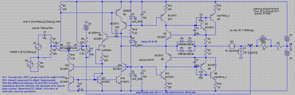
Okay, maybe I should have asked this question earlier, but what exactly constitutes a dangerous response curve?
The peak in my simulations is around 30MHz and 80MHz when using the 2SD/2SB pair. In my simulations, most of those additions except for the 1k resistors had a negative affect and usually caused oscillation. Are we doing things differently somehow?
Some odd observations:
1: With all driver transistors (BD1xx, MJExxx) except for the 2SD/2SB pair, distortion and response went down the tube upon the addition of R10 and R11 (also noted that the BD1xx devices were the worst to use, while the MJExxx ones did fairly well). Is this possible or is it a model error maybe? Using the 2SD/2SB pair, distortion actually went down.
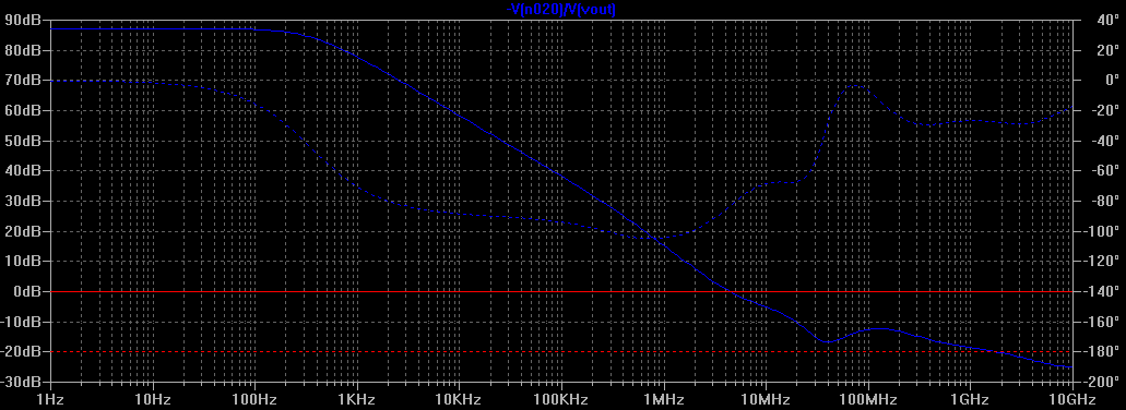
With the following simulation, I got the following response curve:
- keantoken
one pair of plastic packaged 180W devices dissipating 72W of quiescent bias is quite high.
The simulator says they are dissipating about 18W idle each. Bias current is about 1.3A.
Okay, maybe I should have asked this question earlier, but what exactly constitutes a dangerous response curve?
Your output stage has a nasty high frequency response peak around 1 MHz (I think) that would almost certainly cause it the real circuit to oscillate. It took some time to determine why my design didn't have this effect. The final solution was an emitter resistor in the output driver transistors, plus a more conventional Allison frequency compensation scheme - see attached pdf.
The peak in my simulations is around 30MHz and 80MHz when using the 2SD/2SB pair. In my simulations, most of those additions except for the 1k resistors had a negative affect and usually caused oscillation. Are we doing things differently somehow?
Some odd observations:
1: With all driver transistors (BD1xx, MJExxx) except for the 2SD/2SB pair, distortion and response went down the tube upon the addition of R10 and R11 (also noted that the BD1xx devices were the worst to use, while the MJExxx ones did fairly well). Is this possible or is it a model error maybe? Using the 2SD/2SB pair, distortion actually went down.
With the following simulation, I got the following response curve:
An externally hosted image should be here but it was not working when we last tested it.
An externally hosted image should be here but it was not working when we last tested it.
- keantoken
keantoken said:
The simulator says they are dissipating about 18W idle each. Bias current is about 1.3A.
Hi keantoken,
Your rails are +/-24VDC? At 1.3A idle that's 31 watts/device or 72 watts/pair
Keantoken,
I like your current limiting scheme that you show in Post#6. I have now discarded my complex one, and will be using yours. A diagram of my output stage is attached.
I'm using a Bryston style output configuration of four transistors, and a Mosfet driver. The Mosfet seems to help in:
- reducing the THD, by, I assume, not loading the Allison bias transistors, and
- getting a much smoother high frequency rolloff.
The attached stage has very low THD, however I don't expect that the real one will be as good as the simplistic model!
Your current limit scheme will only work if the driver is current limied, otherwise the current limiting diodes will attempt to carry large currents and the VAS transistor will probably die. Email me and I'll describe how to fix this. I'm planning to drive this output stage with an LME49860 opamp, which is current limited to about 45mA.
The Allison bias scheme looks very simple but actually consists of a high loop gain feedback circuit between the output transistors and the bias transistors. This is further complicated if Complementary Feedback Pair (CFP) output transistors are used (a feedback loop inside another feedback loop). Controlling the loop gain is quite important.
AndrewT,
My preferred driver would be (if BJTs where used) the Fairchild KSC2690A/KSA1220A as apart from haing the necessary voltage, current and power ratings, their beta is very constant with current and their Ft is high. I think it is important to use drivers that have an Ft much higher than the output devices, otherwise it is too hard to get a smooth high frequency rolloff.
Mosfets appear to be much better, such as the small Zetex To92's (for a headphone amp perhaps), or the larger irf610/irf9610 To220's. Lateral Mosfets are difficult to use here as there is not enough voltage across the Allison bias transistors.
Paul Bysouth, April 2009
Attachments
Paul,
I think the use of MOSFETs for the Allison has potential for low distortion, since the gate current of the drivers does not decrease input impedance and make it nonlinear (With the exception of the added parasitics). It is the base current of the drivers that makes the input impedance nonlinear, thereby increasing distortion with high-impedance sources.
One minus with using MOSFETs however is that they limit the output swing, for those that worry about it.
I have noted your problem in the simulator. After you posted this, I went in to see what I could do, without limiting the output swing further. This is what I came up with:
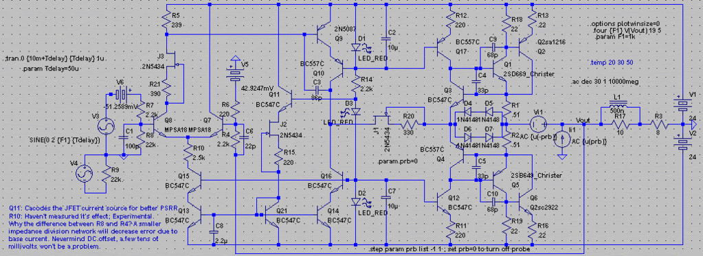
J3 limits the VAS base current (is 6mA too much?) and actually decreases HF distortion somehow (!?). I don't know how good this is, maybe someone will tell me why it's bad. If we use J1, we probably don't need the protection diodes.
Using this also gives a very strange OLG plot!
What does this mean?
As far as stability compensation, I have not had trouble with the Allison the way I have done it on breadboard or simulator, except on more complex versions, where the error was probably my horrible breadboarding skills. I will probably come up with this problem later on when I have the materials necessary, and then I will make the necessary adjustments. I need to start soldering all my experiments.
- keantoken
I think the use of MOSFETs for the Allison has potential for low distortion, since the gate current of the drivers does not decrease input impedance and make it nonlinear (With the exception of the added parasitics). It is the base current of the drivers that makes the input impedance nonlinear, thereby increasing distortion with high-impedance sources.
One minus with using MOSFETs however is that they limit the output swing, for those that worry about it.
Your current limit scheme will only work if the driver is current limited, otherwise the current limiting diodes will attempt to carry large currents and the VAS transistor will probably die. Email me and I'll describe how to fix this. I'm planning to drive this output stage with an LME49860 opamp, which is current limited to about 45mA.
I have noted your problem in the simulator. After you posted this, I went in to see what I could do, without limiting the output swing further. This is what I came up with:
J3 limits the VAS base current (is 6mA too much?) and actually decreases HF distortion somehow (!?). I don't know how good this is, maybe someone will tell me why it's bad. If we use J1, we probably don't need the protection diodes.
Using this also gives a very strange OLG plot!
What does this mean?
As far as stability compensation, I have not had trouble with the Allison the way I have done it on breadboard or simulator, except on more complex versions, where the error was probably my horrible breadboarding skills. I will probably come up with this problem later on when I have the materials necessary, and then I will make the necessary adjustments. I need to start soldering all my experiments.
- keantoken
keantoken said:One minus with using MOSFETs however is that they limit the output swing, for those that worry about it.
Baloney... RDS_on gets you much closer to any rail than VCE_sat.
The only downside, gate charge/discharge cycles have to be
buffered, or higher frequencies drag down input impedance as
seen looking forward through the Aleph/Allison emitters.
And you really don't even need Aleph bootstraps to get there,
though other parts of this circuit can be made simpler if you do.
No need for CCS, rush etc... Just tie em all to the bootstrap.
But let me show you a rail to rail with MOSFETs and no straps,
just to prove that it can be done. Even better if you divide the
output(s) by two before letting Allisons compare backward to
the input. More headroom to play with better mirrors.
The .ASC can be found in my Improving Aleph thread....
Attachments
Well then, I still know nothing about FETs!
I'll let everyone else mess with MOSFETs, but please make a new thread if that's what is going to happen in this one. For now, I want to discuss my circuit and others' ideas/suggestions and I also want to know if there is a better way of overcurrent/VAS protection that can be used without limiting the output swing further.
BTW, what is the simulated distortion of your circuit?
- keantoken
http://www.diyaudio.com/forums/showthread.php?s=&threadid=140114
The above circuit does work (in LTSpice anyway).
The big prob with both Allison (Sziklai) and Aleph (Mosfet)
otherwize identical in this particular context: You can make
class A smooth as glass, none to difficult. But the strong
error correction glitches way too hard when you hit either
rail in clipping and/or AB crossing.
I'll show you a fix for both later.
- Status
- This old topic is closed. If you want to reopen this topic, contact a moderator using the "Report Post" button.
- Home
- Amplifiers
- Solid State
- 50W, Class A, another one... :)