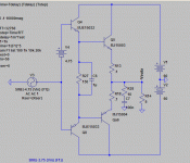
Andy_C mentioned this as a possible topic in the Solid State Spice thread. So, being close to an absolute beginner and not knowing where else to post this, I thought I might start here. I'm building an amp with the LME49810 for the front end and a darlington pair configuration for the current gain section. I would like to test several combinations/configuration of the CG section. So, I need to simulate the output, (maybe without feedback) of the front end. The image below shows what I've done to date.
First, is there a better way? what would that look like?
I would also like to do square wave tests. I've done some previously on full amplifier circuits but with this partial amp, my methodology doesn't work.
First, is there a better way? what would that look like?
I would also like to do square wave tests. I've done some previously on full amplifier circuits but with this partial amp, my methodology doesn't work.
Attachments
You might try using a simple model of a loudspeaker as a load instead of a resistor. This can exacerbate crossover distortion by making the crossover occur at a point other than at zero output voltage.
I think you'll find that you have a DC offset at the output with the circuit as you have it. You should split the bias voltage in two and apply the input to the middle. Note that you will have to readjust the bias for each device you try, to make sure you test them all at the optimum quiescent current.
Also try measuring input impedance (just plot input current against frequency). An output stage might not add that much distortion itself, but it can cause distortion in the VAS by presenting a low impedance, or not sufficiently isolating the VAS from the load impedance.
Modelling speakers is a subject that crops up every so often. Just Re and Le is enough in many cases, but you can add more components for more realistic results.klewis said:I don't know how to make a speaker load... can someone provide me with a sample. I've updated the schematic as suggested regarding the voltage input. See attached.
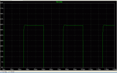
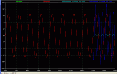
That's a pretty big square wave... is the preceding stage going to be able to swing that wide in the final amp?klewis said:I think I've figured out how to make the square wave work. I used 56v as Vinitial, -56 volts as Von, Trise 1n, Tfall 1n, Ton 2.5e-5 and Tperiod 5e-5. Is this correct for a 10kHz square wave? Enlarged square wave output shown.
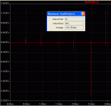
Plot it vs. frequency, like you would for measuring an amp's frequency response. It should end up looking like a normal frequency response graph too, being fairly flat up until some high frequency, then falling smoothly. If you are running the simulation with a reactive load, i.e. a model of a real speaker, then you will see that reflected in the graph too. You can expect the input impedance to be approximately equal to the load impedance multiplied by the output stage's current gain.klewis said:This is the resultant impedance graph and measurement box. Does this look like enought impedance?
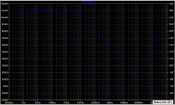
That's better. That will let you see what the VAS will see.klewis said:revised input impedance graph, is this what you expected? I'll look into the other comments...
klewis said:I see that the output voltage swing is 33Vrms. Would that be 33v peak to peak or 66v peak to peak?
For a sine wave, the peak voltage Vp is sqrt(2) * Vrms. The peak-to-peak voltage Vp-p is twice that, or 33 * 1.414 * 2 = 93V
For a square wave, Vrms = Vp, so Vp-p = 2 * Vrms = 66V
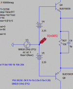
The spec sheet show that the device make a minimum of 6.5mA of output current, how do I show that in the model. Right now, I'm just varying the voltage sources until I get low THD numbers. But I don't know how that coresponds with the bias current. With the input sine voltage set at 46.5v (93/2), the voltate source V4 set at 3v, I measure the current at the base of Q4 and get average of 219uA and RMS of 263uA. I assume that the current is split between Q4 and Q8, but, even so, it's still a factor of ten below the current output. I clearly don't understand what's going on here... thoughts? help.
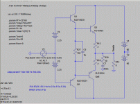
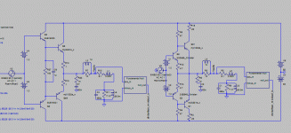
I've added a second model using a CF topology to compare two different OPS(s). I've added a reactive speaker load based upon a single driver in a box using Linkwitz's spread sheet. I believe the design is for a sub. I found the distortion null sub circuit in spice thread, neat tool, but forgot the author's name - sorry. The distortion. I've also added spice models from andy_c's website. Here's the schematic.
Attachments
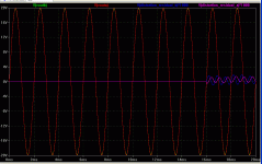
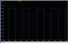
Here's the 10khz plot with 5us delay on outb(CF topology) for visiblity. This plot is with the bias voltage set at 2.6v for both circuits when it's set at 1.16 for the CF, the over shoot is reduced.
I understand that these circuits aren't anything new, I'm not trying to break new ground - not that I could anyway...
Is my methodology (within the constraints of LTspice) acceptable to now try other topologies to compare against these baselines. Could the results of the tests be assumed to be comparable on a relative basis?
Thanks
Ken
Attachments
btw your second output circuit just let out the magic blue smoke. you're feeding PNP output device collectors with the positive rail, and vice versa for the NPN.
i think you have a few things backward in the second circuit. you have your output devices wired backwards C-E for one. recheck that output circuit from whatever source you got it and follow the original schematic exactly.
good thing you did it with the sim and not with physical devices........
i think you have a few things backward in the second circuit. you have your output devices wired backwards C-E for one. recheck that output circuit from whatever source you got it and follow the original schematic exactly.
good thing you did it with the sim and not with physical devices........
- Status
- This old topic is closed. If you want to reopen this topic, contact a moderator using the "Report Post" button.
- Home
- Amplifiers
- Solid State
- Absolute Beginner to SPICE