Your english is fine...jjj84 said:I checked my amplifier speaker outputs for DC and i found +100mV DC.. is this bad? Can it do any damage to my speakers? Amplifier is made of stk4231II.
Is there any way of removing this DC?
ps. sorry bout my bad english, i hope you get the point..
Caps are a possibility, but more than likely you have a differential amp in the input stage that is unbalanced. Solution: Replace input pair transistors. You may match them for optimum results.
My own experiance is that offset of as little as 25mV degrades sound quality noticeably. Others may argue, but I hear what I hear. 100mV is worth tracking down and fixing.
Re: Re: DC-current
In the picture u can see that i cant change those transistors..
In my amplifier input caps are changed from 2.2uF to 10uF, can this cause it? I think not. The amplifier is only 2 months old.
datasheet stk4231II
EchoWars said:Caps are a possibility, but more than likely you have a differential amp in the input stage that is unbalanced. Solution: Replace input pair transistors. You may match them for optimum results.
In the picture u can see that i cant change those transistors..
In my amplifier input caps are changed from 2.2uF to 10uF, can this cause it? I think not. The amplifier is only 2 months old.
datasheet stk4231II
I think we all can conclude this to:
1 How much DC voltage before we get distortion due to displacement of the woofer (not tweeter)?
2 How much DC voltage before a smell can be detected?
1) < 0.5 V (guess), <0.1 V feels good (or safe), <20 mV very OK
2) Depending on how big the woofer is, < 5-10 W I'll guess
100 mV creates a click when the speaker is switched on and off and this can be irritating but hardly harmful for the speaker.
Together with a DC-servo you can reduce the offset to almost nothing, around 1 µV (mean value).
(My new SMD headphone amp with AD8610/BUF634 has only 0.04-0.08 mV at the output! Amazing!)
Now i think that i know where the problem is..
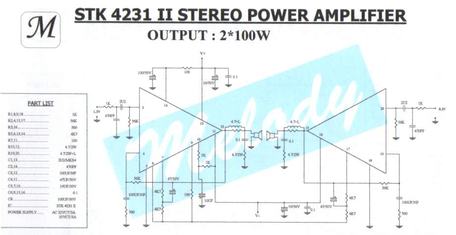
Input coupling capacitors are in the original schematics 2,2uF and the input bias resistors are 56k ohms. This way dc current should be zero.
I my schematic these capacitors are changed to 10uF and the bias resistor is 10k ohms. I think that the reason for this 100mV of dc is caused by wrong value of the input bias resistor.
Does anyone now how to calculate right value for this resistor?
Thanks a lot if someone could help me.
 I would like to help also, but can't find the schematic. Is it somewhere on the net?
Here is the construction manual (in finnish) there you can find the component placement
in this datasheet you can check how the amplifier is made. In my previous post you can find witch capasitors and resistor have been changed
Input coupling capacitors are in the original schematics 2,2uF and the input bias resistors are 56k ohms. This way dc current should be zero.
I my schematic these capacitors are changed to 10uF and the bias resistor is 10k ohms. I think that the reason for this 100mV of dc is caused by wrong value of the input bias resistor.
DC current
You may well be right. Lowering R3 (R4) will decrease the offset at pin 3, but leave the one at pin 4. I would restore R3 to 56k and see if the problem disappears. Alternatively, keep R3 and R9 equal so you have equal input offsets.
But if you lower R9, you should lower R7 also to keep the same gain, and raise C9 to keep the same lf rolloff freq.
Anyway, this amps gain is pretty high (x 100); I guess you really have to be carefull on the volume control. You could just change R9 (R10) to 10K to get a voltage gain of around 20 which should be OK. That way you can leave R3 10k also.
BTW, you didn't say why you changed R3 & C5?
Jan Didden
jjj84 said:
Input coupling capacitors are in the original schematics 2,2uF and the input bias resistors are 56k ohms. This way dc current should be zero.
I my schematic these capacitors are changed to 10uF and the bias resistor is 10k ohms. I think that the reason for this 100mV of dc is caused by wrong value of the input bias resistor.
The resistance from the '+' input to ground should simply be the same as the resistance from the '-' input to the output pin (i.e. if you're following the datasheet circuit, R3=R9, R4=R10). The note at the bottom of p5 mentions this.
This is because each input pin takes a certain amount of DC bias current (the base current of TR1 and TR2 in the schematic). These currents produce a small DC voltage across R3, R4, R9 and R10. Notionally, these bias currents should all be the same, which means if these resistors are the same value, the circuit will be in balance when the output pins are at 0VDC.
If you changed R3 and R4 to 10K because you want a lower input impedance, leave them at 56K but connect 10K across C3 and C4, where they're out of the DC signal path.
The data sheet specs a maximum offset voltage of +/-70mV. If you set R3=R4=R9=R10 and it's still outside this range, you either have a fried chip, or some other component could be out of spec.
100mV offset is not likely to damage the average speaker, but worth fixing to make sure there's nothing else wrong with your amplifier.
Cheers
IH
") Thanks in advance, have you by the way solved the problem?
Thanks in advance, have you by the way solved the problem?- Status
- This old topic is closed. If you want to reopen this topic, contact a moderator using the "Report Post" button.
- Home
- Amplifiers
- Solid State
- DC-current