hello..
i am a newbie in the forum.
reasonably at ease with electronics and working hands on..
built a couple of chipamps based on 1875 and 3886.
Now i want to build a SS power amp.
I have read Randy sloanes and douglas self books on the topic
i wanted to design a small/ medium power amplifer myself as i think it ll be better for my own understanding of the subject..
the amp is based on Linn topology and draws heavily from sloanes teaching ( i think it is far easier)
as in Lin topology i wanted to first design the three stages individually.
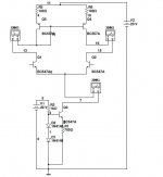
attached below is my first attempt at designing the input stage
i am facing several problems with the design.
1. The current source is not sinking 1 ma as designed.
2. The mirror is not effective
Initially the sink current starts off from 220 Ua and the current is evenly split btw the mirror arms.
after sometime(abt a min) the sink current reduces to 40 Ua and the current is not matched. the current in the arms differs by 3-4 Ua.
and slowly the sink current reduces to 0.
I am able to understand the working based on tested designs of sloane and debug it ,but am not able to design a simple one myself.
Help please...!!
i am a newbie in the forum.
reasonably at ease with electronics and working hands on..
built a couple of chipamps based on 1875 and 3886.
Now i want to build a SS power amp.
I have read Randy sloanes and douglas self books on the topic
i wanted to design a small/ medium power amplifer myself as i think it ll be better for my own understanding of the subject..
the amp is based on Linn topology and draws heavily from sloanes teaching ( i think it is far easier)
as in Lin topology i wanted to first design the three stages individually.
attached below is my first attempt at designing the input stage
i am facing several problems with the design.
1. The current source is not sinking 1 ma as designed.
2. The mirror is not effective
Initially the sink current starts off from 220 Ua and the current is evenly split btw the mirror arms.
after sometime(abt a min) the sink current reduces to 40 Ua and the current is not matched. the current in the arms differs by 3-4 Ua.
and slowly the sink current reduces to 0.
I am able to understand the working based on tested designs of sloane and debug it ,but am not able to design a simple one myself.
Help please...!!
Attachments
First, set the diode current at 1mA by changing R2 to 20K. Make sure the diodes are still good. At 1mA they should each have 0.6V across them. Change R1 to something close to 600 ohm.
You must have a DC bias source for both transistors in the diff pair. 47K to ground will give you that bias so you can check operation.
You must have a DC bias source for both transistors in the diff pair. 47K to ground will give you that bias so you can check operation.
krish2487 said:@steve dunlap and @ tze yang
thank you..
it did work
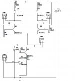
i am posting the updated version
the mirror is accurate to the seconf decimal in ma.
")
sink current is set to , as u can see, about 100ma
thank you again.
It looks more like 60mA. That puts the transistor dissipating 1.2W. You might want to lower that by at least a factor of 10.
R2 is still low. Try setting the diode current at 1mA.
Hi
Q1 & Q2 bases need to have a voltage potential of half Vcc or +10V. (GND, 0V if you use +/-10V supply) This is where the input and feedback (-input) nodes will be. If they are tied to the positive supply, there will be no Vce left for Q1 & Q2. Base voltage level can be set with voltage divider bias or GND of a split supply.
BC547 has lots of current gain so base current shouldn't be more than a couple of uA. (BTW C grade is the highest gain class and A grade is the lowest.)
The idea of the mirror is to split the current and keep Ic of both sides equal.
Forward voltage drop of one diode and Vbe of the transistor should be about the same. So 1 forward PN juction voltage (0.6V) is left across R1. Also you can research
2 transistor CCS and self bias J-fet CCS.
Emitter degeneration may be needed for Q1 & Q2 unless you go to specific lengths to match them.....or buy a matched transistor array, probably more expensive. The emitter resistor will make the % difference in the transistor variables less, at the expense of some gain. It's a good trade-off.
@ steve , cbs240, andrew
thank you..
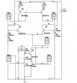
the updated version is attached below..
the bases of the input transistors are at 9 v approx.
the sink current is at 1.5 ma split evenly between the arms and mirrors excellently.
it has a been a big help from you all
atleast my fundas are falling into place now..
thank you..
the updated version is attached below..
the bases of the input transistors are at 9 v approx.
the sink current is at 1.5 ma split evenly between the arms and mirrors excellently.
it has a been a big help from you all
atleast my fundas are falling into place now..
Attachments
- Status
- This old topic is closed. If you want to reopen this topic, contact a moderator using the "Report Post" button.
- Home
- Amplifiers
- Solid State
- Help with designing differential amplifier