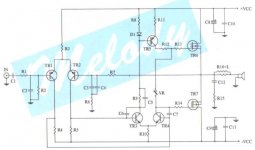
your schematic
has absolutelly no info .....
....to a schematic like that ( meaning that simple ) everything or almost everything may cause an ammount of distortion
the first stage will easilly work better with a ccs
c6 vas capacitor if not calculated properly depending on layout transistor selection rail voltage and many others could be a "sonic " killer and so on and on and on ....
it could be everything ..... so give us a proper schematic and others will give you far more sophisticated comments
To be honest this circuit isn't particularly good. No emitter degeneration in the LTP, no proper current source for the LTP.
To be honest if you want a simple, good Lateral MOSFET amp, Rod Elliot's P101 is a good place to start. Personally I would replace the bootstrap with a current source, but that is just me.
If you're trying to use vertical MOSFETS (IRF types) with this circuit though, forget it... it won't work properly and eventually the outputs will overheat. If that's the sort you want to build, start by looking at Quasi's NMOS amps.
rtill said:what would cause distortion in this circuit? is the bias not adjusted correctly?
It sounds powerful and great, but there is faint distortion.
The short answer is that it is TIM waiting to happen and it's 20 kHz THD is probably awful. It also likely has rather low slew rate.
To begin, the use of an un-degenerated BJT input LTP is a big no-no that should have vanished from design practice in the early 1970's if not sooner.
Secondly, I strongly believe that it is foolish to try to drive output MOSFETs directly from the VAS. An EF driver/buffer stage should be put in between. Some people will disagree with me on this point, however. Just because MOSFETs have "infinite" DC beta does not give the designer license to drive them directly from the VAS.
Sadly, this is the kind of simpleton design that some well-intentioned audiophile designer will fill with very expensive capacitors and think it then sounds better. Oh, I forgot the fancy milled aluminum front panel, the blue LED and the $5000 price tag.
Cheers,
Bob
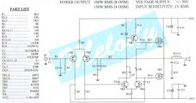
You might find a few pointer s in my amp cct.
An externally hosted image should be here but it was not working when we last tested it.
Trill, you seem to have come across the "melody" collection..
I have a dozen or so of these and besides being written in
either greek or russian , they are basic "schoolbook" designs
and should be used accordingly . Even the melody BJT designs
are unproven and prone to thermal runaway / and
or oscillations. quasi or ESP designs have been "built to death"
with support...better in the long run (for your speakers).
The gate capacitance of the OP stage will degrade/affect the Cob
of the VAS...an MJE340/350 EF after the VAS will be highly
beneficial, distortion/stability wise.
OS
OS
I have a dozen or so of these and besides being written in
either greek or russian , they are basic "schoolbook" designs
and should be used accordingly . Even the melody BJT designs
are unproven and prone to thermal runaway / and
or oscillations. quasi or ESP designs have been "built to death"
with support...better in the long run (for your speakers).
Secondly, I strongly believe that it is foolish to try to drive output MOSFETs directly from the VAS. An EF driver/buffer stage should be put in between. Some people will disagree with me on this point, however. Just because MOSFETs have "infinite" DC beta does not give the designer license to drive them directly from the VAS
The gate capacitance of the OP stage will degrade/affect the Cob
of the VAS...an MJE340/350 EF after the VAS will be highly
beneficial, distortion/stability wise.
OS
OS
Hi Richard,
I am surprised at some of the comments you received. Firstly if your LPT is well matched, degeneration resistors increases distortion.
There is nothing uncommon about driving lateral mosfets from the VAS, it works fine.
The amplifier performs well at high frequency and at 100kHz range at full power, THD is a not too shabby 0.12% and at 1 kHz it is around 0.006% better than most.
TIM is not lurking around the corner waiting to mug you. The phase response is ruler flat throughout the audio band with only -8 degrees at 100 kHz there are many high class designs that is three to four times this high.
The slew rate is > 28V/us and better than most. There is no notable over or undershoot using square wave.
In my opinion there is absolutely nothing wrong with your simple amp and if you like what you hear then that is what it is all about enjoying your music.
Kind regards
Nico
I agree driving vertical mosfets from the VAS isn't a good idea.
But the laterals have only 10pf or so of Ggd
The Cgs is the limiting factor - limiting current slew rate. But aren't speakers inductive at high frequencies? Current slew rate needed for a certain voltage slew rate will be lower than that needed by a totally resistive load.
But the laterals have only 10pf or so of Ggd
The Cgs is the limiting factor - limiting current slew rate. But aren't speakers inductive at high frequencies? Current slew rate needed for a certain voltage slew rate will be lower than that needed by a totally resistive load.
Maybe this topology is inspired by Jean Hiraga's amp http://www.tcaas.btinternet.co.uk/monster27f.htm Revert PNP to NPN, it's diagram is similiar to the diagram in pic.1 lower left
Bob Cordell said:Sadly, this is the kind of simpleton design that some well-intentioned audiophile designer will fill with very expensive capacitors and think it then sounds better. Oh, I forgot the fancy milled aluminum front panel, the blue LED and the $5000 price tag.
Cheers,
Bob
This is why mosfet amps 'sound bad' to many audio enthusiasts. But, of course with that fancy case and pretty blue LED in there......WOW! Awsome.

You might find a few pointer s in my amp cct.
One thing about using a pot for emitter resistors to set the DC output bias at the LTP is that if it is not centered, then the degeneration (local feedback) of each element in the LTP is different. It is important, IMHO
 , to have not only the DC components of the LTP equal, but also the AC parts as well. IMO, it would be better to have fixed emitter resistors and a pot in series with the emitter resistor of Q3 to adjust the LTP tail current for DC offset.
,


megajocke said:I agree driving vertical mosfets from the VAS isn't a good idea.
But the laterals have only 10pf or so of Ggd
The Cgs is the limiting factor - limiting current slew rate. But aren't speakers inductive at high frequencies? Current slew rate needed for a certain voltage slew rate will be lower than that needed by a totally resistive load.
Cgs might be substantially greater, but it is essentially bootstapted because the outputs are followers and G-S voltage has little variation.
However, the output stage presents a nonlinear loading to the VAS(especially in the crossover region) and that should be minimized IMHO.
This must be a really BAD amp.
An externally hosted image should be here but it was not working when we last tested it.
Efficency will be BAD... 
Distortion might not be as it's pure class A.
The originally discussed circuit can be seen in an application note from Hitachi that accompanied the lateral mosfets. (could have been upside down with NPN input though, I don't remember) Performance is surprisingly good for such a simple circuit!
Distortion might not be as it's pure class A.
The originally discussed circuit can be seen in an application note from Hitachi that accompanied the lateral mosfets. (could have been upside down with NPN input though, I don't remember) Performance is surprisingly good for such a simple circuit!
- Status
- This old topic is closed. If you want to reopen this topic, contact a moderator using the "Report Post" button.
- Home
- Amplifiers
- Solid State
- distortion...mosfet