they are great, almost bomb proof.
i have run them into 4 ohms aswell and they held up ok.
less than 0.01% distortion, more than good enough for disco work.
only had a pair of bridge rectifiers blow in about 20 years, and that was from a pint of larger in a speaker!! even the output mosfets where ok! oh how i hated 18th birthday partys!
steve.
Lateral type mosfets are pretty hard (= almost impossible even if trying) to destroy...
I didn't expect a 2SJ50, rated 100W at 25 degrees C case temperature to survive 200W dissipation at 100 degrees C case temperature for any longer than a couple of seconds but it did I think I had it running at 200W and 100 degrees case temperature for over a minute total. Still works! (if the suggested thermal resistance in the datasheet is correct that would mean a junction temperature of at least 300 degrees C)
The problem with low load impedances isn't very likely to be destruction but power-reducing things like a lot of voltage drop at high currents (up to 15V) and a current limit that decreases with temperature.
I didn't expect a 2SJ50, rated 100W at 25 degrees C case temperature to survive 200W dissipation at 100 degrees C case temperature for any longer than a couple of seconds but it did
I think I had it running at 200W and 100 degrees case temperature for over a minute total. Still works! (if the suggested thermal resistance in the datasheet is correct that would mean a junction temperature of at least 300 degrees C)The problem with low load impedances isn't very likely to be destruction but power-reducing things like a lot of voltage drop at high currents (up to 15V) and a current limit that decreases with temperature.
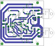
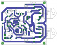
just incase any one is interested i did a quick rework of the old pcb board and came up with this...
it may need a little tweeking, but it looks ok to me. also dont pay attention to the names and numbers i only did it as a layout plan.
cheers guys, steve.
it may need a little tweeking, but it looks ok to me. also dont pay attention to the names and numbers i only did it as a layout plan.
cheers guys, steve.
Attachments
Lateral mosfet pinout is G S D, not G D S like on verticals so you need to change the layout.
I also suggest you separate signal ground and decoupling ground on board to make it easier to get a hum, distortion and cross-talk free amp.
Decoupling ground making a loop around the whole card isn't best but might be good enough. Better would be if it can be routed to the right of the mosfet pins.
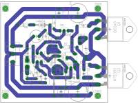
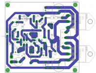
hows this look??
re pinned the outputs and added resistor from signal ground, may make it a cap or leave out res and take it back to star point.
just my thoughts on it, and i may make a pair to see, but i like the look of the earth decoupling, not sure about a ground loop, its not a full circle (not joined at the other end) and keeps both lines a more equal length, so it may be good.
cheers, steve.
Attachments
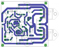
The feedback DC blocking cap, input HF filter cap and resistor from input to ground should be on the signal ground side of the separation.
The power supply/ground routing may not be as important but having them going around the board like that isn't optimal - half wave currents in the supplies will create magnetic fields going through the small signal circuits.
The reason I'd run decoupling ground and put power inputs near the power transistors is that I want the lowest possible supply inductance as seen from the output stage (where it matters) and want to keep negative and positive half waves close to each other (which makes emitted magnetic fields non-distorted) - not because of "ground loops"
But the separation of signal and power ground and which connections belong to which is much more important than those effects.
Look at this link for an amp with similar power supply layout and the fix needed to lower THD which was higher due to the layout:
http://www.lf-pro.net/mbittner/Sym5_Webpage/symasym5.html
"Placing a short thick wire connecting the ground pins of the supply caps reduces THD"
edit:
Looks like something is wrong with the jumpers connecting the VAS stage to supply at the bottom of picture.
I dont want to be fussy BUT if your going to totally rebuild the GA28f amplifier you are really missing something if you don't add a constant current source for the input pair where R3 is on your schematic.
There of course many different improvements that can be made to this circuit and it is basically sound.
I own 2 Maplin stereo 150 w amps, 3 BK Electronic amps, a C-audio SR707, and a Rauch DVT 50 and they are all basically the same circuit with different add ons.
Adding a constant current source improves the power supply rejection, which may be relevant to you if you are going to run multiple amps on a single supply.
sounds good, i didnt intend to rebuild the amp, just change to t03p case mosfets, but since were here, might aswell go the some of the way with the c c s for the input pair.
i'll have a look and play with the schem and post back when i have something.
yes quite alot of the amps from around the same era are just the same design with tweeks. i cant think of any right now but from memory some of the H + H are similar, as are some of the carlsbro amps, but then i think carlsbro ended up buying H+H so that isnt a surprise.
cheers guys, steve.
kevvywevvywoo said:I have a commercial power amp here using the 2sJ200 / 2sk1529 and the output pair on one side have gone s/c. Given that these originals are obsolete, what can you recommend as viable, reliable replacements that won't be likely fakes?
How many pairs of 2sJ200 / 2sk1529 do you want?
ok so what is better to use??
diode fed constant current source?
or, twin transistor ccs?
or, a transistor capacitance multiplier?
ive done the last one before in an amp power supply, so ive done a quick layout with that one, see what you think.
cheers, steve.
diode fed constant current source?
or, twin transistor ccs?
or, a transistor capacitance multiplier?
ive done the last one before in an amp power supply, so ive done a quick layout with that one, see what you think.
cheers, steve.
Attachments
A favorite seems to be the diode fed CCS using a green LED that drops about 2V.
Although I have a bias towards using a 2 transistor CCS as the Rauch DVT as this amp performs very well.
The current needs to be about 1mA.
Excuse me if I’m wrong but is a capacitance Multiplier the wrong thing to use here.
The input pair is just above 0v and so R3 in your original circuit is dropping 50 V across 47K so approx 1mA.
- Status
- This old topic is closed. If you want to reopen this topic, contact a moderator using the "Report Post" button.
- Home
- Amplifiers
- Solid State
- replacement mosfet recomendations??