Hi there,
I've already touched on this in my amp design thread but I've been trying to study the phenomenons of cross-conduction and rail sticking, mainly with respect to my own amp design. While there are odd bits of information dotted around the forum I couldn't find much discussing what factors cause it and how to mitigate it.
From my own simulation experiments I have observed the following:
I know it is impossible to avoid entirely but because of the application I'm designing for I would like to make sure that occasionally driving the output stage into clipping will not cause immediate destruction of the amplifier.
I'm sure I can't be the only person who would be interested in this discussion...
I've already touched on this in my amp design thread but I've been trying to study the phenomenons of cross-conduction and rail sticking, mainly with respect to my own amp design. While there are odd bits of information dotted around the forum I couldn't find much discussing what factors cause it and how to mitigate it.
From my own simulation experiments I have observed the following:
- Occurs mainly when the amplifier output is moving away from a supply rail during overload conditions
- Is caused when the NFB tries to correct for the output stage not reacting quick enough, thus causing eg the negative side output devices to turn on before the positive side has turned off
- Seems to affect all output topologies (that I've tried) similarly
- In my case, affects the positive side more than the negative
I know it is impossible to avoid entirely but because of the application I'm designing for I would like to make sure that occasionally driving the output stage into clipping will not cause immediate destruction of the amplifier.
I'm sure I can't be the only person who would be interested in this discussion...
Thanks for that. I knew it had something to do with saturation of the devices but now I know what to search for.
I thought I tried running the drivers with plenty of current and less current without noticing a huge amount of difference. I should redraw my test amplifier and do some more detailed experiments though. I've completely hacked the schematic in Orcad by trying different topologies and even adding totem-pole drivers to suck the charge out. Interestingly the problem seems to be mainly with the driver transistor rather than the output device.
For the positive side I'm using an MJE15033 driven by a BF422 in a CFP (Sziklai) configuration which drives into a parallel pair of the new ONSemi Thermaltrack NJL1302 output devices
Schematic has changed slightly but it's basically this: http://www.chaudio.co.uk/AmpDesign/Amp1ProtoSchematic.pdf
ceharden,
at first I feared that the problem was more serious (CFP output stage). Lowering the value of R6 will speed up the discharge of Q16 base and give a desirable higher quiescent current but requiring a stronger device for Q6, which can easily cause instability. The high rail voltages complicate proper biasing. Your design looks OK to me, I would not add totem-pole drivers.
roender,
Exactly.The cross conduction phenomena is closely related with minority carriers accumulation in base emitter junctions. In your schematic, drivers are connected to output node. Please avoid that if you use CFP drivers configuration.
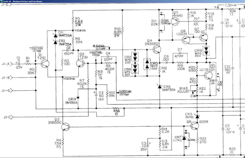
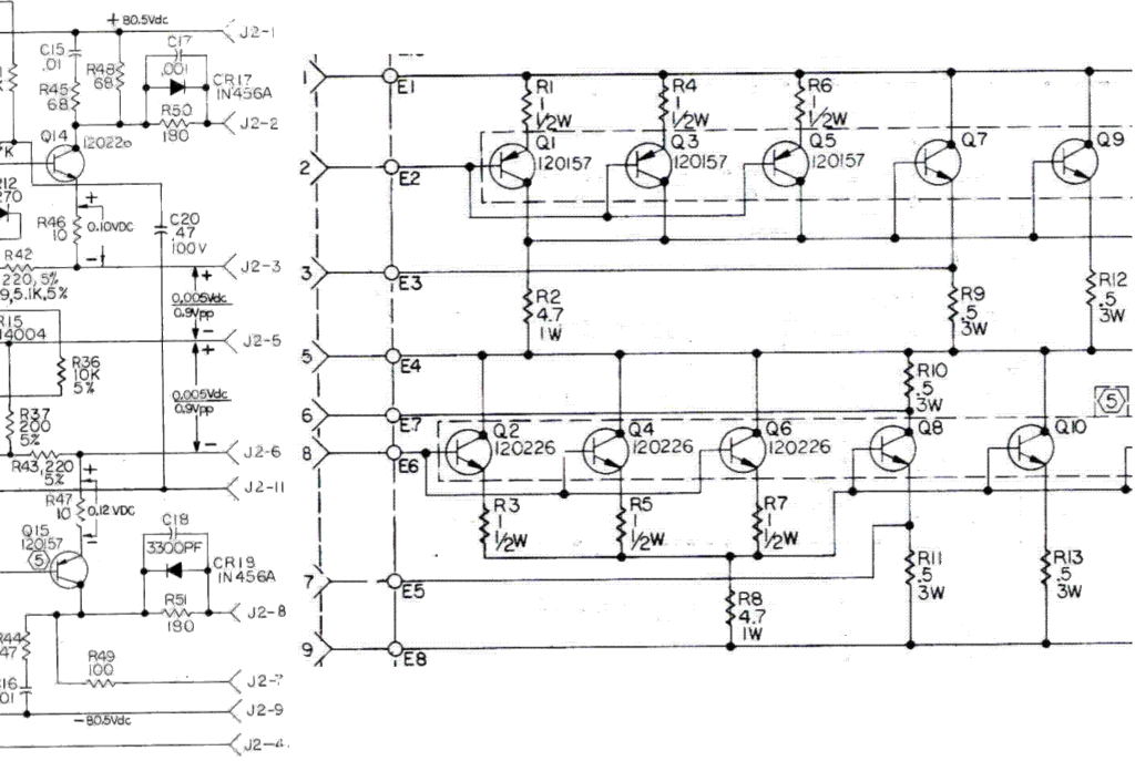
Perhaps these Altec 9440 schematics will be of some help.
The amplifier is quasi, but could be easily made complementary. Please note the diodes around Q7 and Q8. They prevent driving the output stage into saturation.
http://i56.photobucket.com/albums/g196/dkleitsch/9440-12.jpg
Also note the values of the resistors around the CFP and outputs.
The amplifier is quasi, but could be easily made complementary. Please note the diodes around Q7 and Q8. They prevent driving the output stage into saturation.
An externally hosted image should be here but it was not working when we last tested it.
http://i56.photobucket.com/albums/g196/dkleitsch/9440-12.jpg
Also note the values of the resistors around the CFP and outputs.
ceharden said:Thanks for that. I knew it had something to do with saturation of the devices but now I know what to search for.
I thought I tried running the drivers with plenty of current and less current without noticing a huge amount of difference. I should redraw my test amplifier and do some more detailed experiments though. I've completely hacked the schematic in Orcad by trying different topologies and even adding totem-pole drivers to suck the charge out. Interestingly the problem seems to be mainly with the driver transistor rather than the output device.
For the positive side I'm using an MJE15033 driven by a BF422 in a CFP (Sziklai) configuration which drives into a parallel pair of the new ONSemi Thermaltrack NJL1302 output devices
Schematic has changed slightly but it's basically this: http://www.chaudio.co.uk/AmpDesign/Amp1ProtoSchematic.pdf
Try a 0.1-1uF capacitor between bases of the output stage devices.
Still I agree that the best way is to prevent output stage from saturation by using clamping at VAS with fast diodes. Forget about those switched-mode-half-bridge tricks, it is not the way here.
Regards, Adam
Thanks again for the input.
djk, I'm having some trouble reading the schematics you posted. The jpeg compression seems to have made the component numbers and values illegible.
I'm trying to run the driver stage a bit hotter which does seem to help. The figures coming out of the simulation are a bit scary with peak output device dissipation easily exceeding 1kW in some cases.
One cheat seems to be to run the input stage at a slightly lower voltage than the output. Just 1V lower is enough to reduce the saturation of the output stage.
Of course now, all this messing around with the circuit means that my distortion performance isn't so good! Damnit!
Here's a new schematic, not perfect but at least some of the problems fixed. http://www.chaudio.co.uk/AmpDesign/Amp1SchRev2.pdf
cross conduction (a.k.a. common mode conduction) has a close relarionship to output device beta and Ccb (Miller capacitance). try reducing the beta in your transistor model to the low side of the beta range for the transistor. my guess is that the beta in your model is at "design center" or higher. when you build an amp for real, try selecting devices between the minimum and "typical" values on the spec sheet.
djk: Thanks for reposting the images, I can see what you're on about now. I'll have a play in the simulations and see how it works for me.
By the way, how close to the supply rails is it normal to be able to get an amplifier output to run. With my +/- 65V rails (likely to be going up slightly because I've found a better transformer lying around) I'm able to get up to +/- 58-60V peak voltage swing. Is this about normal?
unclejed: That's useful to know, thank you. Using that info it turns out that the Thermaltrak devices I'm using in the real amp are in theory even worse than the MJ15022/23's I'm using in the simulation (slightly higher Cob and definitely higher hfe).
I'm yet to work out a good way of trying to detect/measure cross-conduction in the real amplifier. My scope isn't accurate enough in differential mode to monitor the voltage across the output emitter resistors. I need an isolation amplifier or something. Although I can run the amp floating still don't want to connect the scope ground to anything other than a ground connection!
If you're getting about a 6 volt minumum VCE in your outputs, the VAS is likely limiting the swing - not the outputs. This is normal - and in most topologies suitable for high power it does. You won't get enough cross conduction to be a problem unless you're planning on running continuous clipping at several hundred kHz. With most modern output transistors you can clip the *** out of it and not see a problem. With emitter followers or CFP and limit occuring in the VAS, you won't get much if any increase in current with continuous clipping without a load. Depending on the VAS design you could get rail sticking, but that's only a SQ issue not a destruction issue.
the way we used to test for cross conduction was to run the amp full input (1.5vrms) at 100khz, no load and watch the line current on the variac. the primary side of the amp supply was fused for 5 amps. if the fuse blew after a 5 sercond test, the amp failed the cross conduction test. it was a rather crude test, but it was effective at catching output devices that were out of spec.
actuall the best way to detect cross conduction would be to use toroid cores around 1 each of + and - side emitter resistors with several turns of wire as a current probe. the emitter resistor acts as a single turn primary, and your secondary turns feed scope inputs or an ac millivoltmeter.
actuall the best way to detect cross conduction would be to use toroid cores around 1 each of + and - side emitter resistors with several turns of wire as a current probe. the emitter resistor acts as a single turn primary, and your secondary turns feed scope inputs or an ac millivoltmeter.
If the light bulb stays off when driving 6dB into clip at 50KHz with no load I call it good and move on. I haven't seen a cross conduction problem in a complimentary output stage - ever. Last one that I had a problem with was back in 88 or 89 - with an all NPN stage using paralleled 2N5631's. Same thing with hometaxial 2N6259's didn't like HF any more, but at least it survived the torture. Same front end with D424/B554 didn't draw any undue current.
I think what you're trying to say politely is stop worrying and get on with it!
What I've realised is that the duration of the cross conduction pulses I'm seeing in the simulations are actually very short. I've been simulating with a 1kHz sine wave. The cross-conduction lasts for less than 1/20 of a cycle. That's 500us or actually much less if you just look at the bit that's outside of the transistors rating. Plus the other factor is that I'm simulating with a 'stiff' power supply. In a real amp there are probably extra resistances which will limit the peak current.
So maybe the verdict should be that as long as I'm taking the usual sensible steps to avoid it, I'm looking at a problem which isn't one in practice.
I'm planning for the ultimate amp on the design board to have a fairly clever clip/current limiting strategy anyway but just wanted to be sure that the amp would survive mild clipping without it.
I'm also looking at changing some of my BF422/423's for MJE340/50's to give higher current capability.
Our member Edmond made a clever way to overcome this. In his "PMP" amp, he make a clamp that send a signal back to inverting input when the output stage is near clipping. This reduces the amp's OL gain. I think this solves the core of the problem.
Attachments
I use MJE15032/33 drivers with 80mA bias, and 1uF capacitor between the emitters to drive 4 pairs of MJL21193/94. I never found any cross conduction.
But this is the maximum number of output devices it can handle. For 6 pairs, I used another pairs MJEs, and increase the current up to 120mA.
The best limiter I found is in the ML amplifiers, with dedicated network. That works quite good!
Sajti
But this is the maximum number of output devices it can handle. For 6 pairs, I used another pairs MJEs, and increase the current up to 120mA.
The best limiter I found is in the ML amplifiers, with dedicated network. That works quite good!
Sajti
- Status
- This old topic is closed. If you want to reopen this topic, contact a moderator using the "Report Post" button.
- Home
- Amplifiers
- Solid State
- Cross-conduction - how to avoid?