Well here I go again... I just can't stop drawing and thinking amps. This is my latest thinking for what I am going to build next. I *almost* caved and used a P-channel fet on the bottom but I came to my senses ") at the last moment. Now ordinarily I don't like quasi complementary output stages because the lower transistor / fet has somewhat higher gain, particularly if you have a mosfet output stage. Actually the overall voltage gain is the same, just the tansconductance is way higher, leading to assymetrical feedback. When I have my amps running I like to go "mmm....." and luxuriate in the thought of all that electronic niceness happening. But if the thing is just a can of worms beaten into shape by brute force feedback; well no thanks.
at the last moment. Now ordinarily I don't like quasi complementary output stages because the lower transistor / fet has somewhat higher gain, particularly if you have a mosfet output stage. Actually the overall voltage gain is the same, just the tansconductance is way higher, leading to assymetrical feedback. When I have my amps running I like to go "mmm....." and luxuriate in the thought of all that electronic niceness happening. But if the thing is just a can of worms beaten into shape by brute force feedback; well no thanks.
What I have done in this design is make the bipolar on the lower fet have a gain of only 1. (equal emitter and collector resistors) This means that a -1 volt change in base voltage make the same increase of drain current as would a +1 volt increase of gate voltage on the upper fet. This means we have a pretty close approximation of a real p-channel fet, not one with ridiculously high transconductance that is hopelessly mismatched to it's upper counterpart.
I did a quicky test of the output stage only with no load this afternoon and the rise and fall time was 700nS almost exactly with a 20v p/p square wave output. I think it is mostly limited by the gate resistors whch could probably go as low as 100 ohms, but the thing is still pumping out an 18 volt p/p sinewave at 250kHz so I wasn't really fussed.
The input part with the LM317 regs is covered in this thread -> http://www.diyaudio.com/forums/showthread.php?s=&threadid=13215&perpage=15&pagenumber=1
The cct still needs temperature compensation of the bias, and a dc servo feedback thingy to eliminate any dc offset voltage at the output. The bias voltage is applied in such a strange way so that the lower fet can get it's gate pulled up even when it's drain is right down at the lower rail, otherwise there would be no voltage available the the PNP's emitter to give any gate drive. Still needs a bit of work though I feel. The upper fet's gate drive is floating too so the thing will swing from rail to rail. Amps that can't do this are something of a pet peeve with me BTW.
Anyway, I've only just started this thing and so it will evolve as time goes on. As always, I invite your points of view and criticism. Just dont try and talk me out of LM317's and quasi complementary. This amp is gunna have personality.
at the last moment. Now ordinarily I don't like quasi complementary output stages because the lower transistor / fet has somewhat higher gain, particularly if you have a mosfet output stage. Actually the overall voltage gain is the same, just the tansconductance is way higher, leading to assymetrical feedback. When I have my amps running I like to go "mmm....." and luxuriate in the thought of all that electronic niceness happening. But if the thing is just a can of worms beaten into shape by brute force feedback; well no thanks.What I have done in this design is make the bipolar on the lower fet have a gain of only 1. (equal emitter and collector resistors) This means that a -1 volt change in base voltage make the same increase of drain current as would a +1 volt increase of gate voltage on the upper fet. This means we have a pretty close approximation of a real p-channel fet, not one with ridiculously high transconductance that is hopelessly mismatched to it's upper counterpart.
I did a quicky test of the output stage only with no load this afternoon and the rise and fall time was 700nS almost exactly with a 20v p/p square wave output. I think it is mostly limited by the gate resistors whch could probably go as low as 100 ohms, but the thing is still pumping out an 18 volt p/p sinewave at 250kHz so I wasn't really fussed.
The input part with the LM317 regs is covered in this thread -> http://www.diyaudio.com/forums/showthread.php?s=&threadid=13215&perpage=15&pagenumber=1
The cct still needs temperature compensation of the bias, and a dc servo feedback thingy to eliminate any dc offset voltage at the output. The bias voltage is applied in such a strange way so that the lower fet can get it's gate pulled up even when it's drain is right down at the lower rail, otherwise there would be no voltage available the the PNP's emitter to give any gate drive. Still needs a bit of work though I feel. The upper fet's gate drive is floating too so the thing will swing from rail to rail. Amps that can't do this are something of a pet peeve with me BTW.
Anyway, I've only just started this thing and so it will evolve as time goes on. As always, I invite your points of view and criticism. Just dont try and talk me out of LM317's and quasi complementary. This amp is gunna have personality.
Attachments
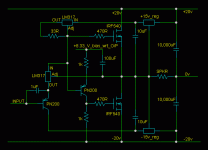
Late night drawing mistake.
The inputs to the + / - 15v regs is meant to go to +/- 20v dc rails floating separate from the main rails. The common connection for these regs also goes to the zero V connection of this floating supply, as well as the live spkr output connection as shown.
The inputs to the + / - 15v regs is meant to go to +/- 20v dc rails floating separate from the main rails. The common connection for these regs also goes to the zero V connection of this floating supply, as well as the live spkr output connection as shown.
Circlotron said:Well here I go again... I just can't stop drawing and thinking amps.
...Downright healthy attitude to have....

Righteo then. First of all, I set the supply rails to + / - 15 volts while I was testing to limit the size of the potential explosion  but there was no drama. Later on I will put it up to about + / - 42 volts with the transfomer I have. My goal is 100 watts into 8 ohms. Seeing I can drive the mosfet gates outside the rails this should not be too much of a problem to go practically rail to rail. Most amps can drive the gates to the rails at best, so the sources only go to within perhaps 5 or 6 volts from the rails then this limits the power output somewhat. Seeing the power output depend on the *square* of the output voltage, this last couple of volts can make a worthwile improvement to the output.
Anyway, the sig gen could only manage 20v p/p so seeing the amp is only a buffer at the moment the output was likewise limited to 20v p/p. (Life really is tough sometimes). I set the bias so the quiescent current was 400mA to get out of the curviest part of the gate voltage -> drain current curve. Sine wave in and hey presto! sine wave out. Clean as you like. Triangle wave looked pretty good too. Square wave had a bit of ringing but in fairness the input signal had a 10nS rise and fall time! In real life it will be driven from a CD player analog output, so a 20kHz full power sinewave is about as bad as it gets IMHO. Anyone care to offer another opinion there?
I had the use of an HP34401A 6-1/2 digit dmm http://we.home.agilent.com/cgi-bin/...36880933.00&LANGUAGE_CODE=eng&COUNTRY_CODE=ZZ at my bench at work (I would recommend one of these to anybody - expensive but excellent) and measured the ac output voltage (these meters have a GOOD frequency response) of the amp at no load and with a 6 ohm resistive load and noted any change. At 1kHz the output was 7.1139 volts RMS dropping to 7.1027V at 6 ohms, a drop of 11.2 mV. At 20kHz it was 7.1102V to 7.0984V, a drop of 11.8 mV. That works out to an output impedance of 0.00944 ohms at 1kHz. Yay! Also, with regard to the thread on null testing http://www.diyaudio.com/forums/showthread.php?s=&threadid=13415 I got the meter and put one lead on the input and the other on the output (only valid for non-inverting amps with X1 "gain") to measure any difference between input and output. Typically there was about 2.1 mV under load. Not sure what that would approximate in distortion figures, but at least it means things ain't misbehavin'.
For frequency rsponse flatness, as mentioned, the output was 7.1027V at 1kHz, dropping to 7.0984V at 20Khz. How many dB is that? Still have to fiddle a bit with the lower mosfet gate drive. I'm still not happy that I will get enough peak gate voltage at high levels. Also I might put a pot in place of the emitter resistor of the BJT driving the lower mosfet. That way I can tweak the BJT gain to exactly X1. At the moment under full output into the load I measured 420 mV into the upper gate and 424 mV into the lower gate. No big deal, but this is diy don't forget!
Anyway, I'm really pleased so far. It has shown none of the bad manners and snapping and snarling like the "Circlotron Doomsday Amplifier" that I wrestled with some time ago. http://www.diyaudio.com/forums/showthread.php?s=&threadid=3891 That thing was a paragon of blood and fire and columns of smoke, of lightnings and thunders and voices, a thing to be feared. Well actually it was a bit of a nuisance more like it, although it did work quite well between blowups.
So, what I have to do now is cook up some kind of front end for it that will swing say + / - 45 volts into maybe 10k impedance. Probably some other normal power amp cct all the way up to the output device bases. And get the bias temp compensation working too. Lotsa work, lotsa fun.
but there was no drama. Later on I will put it up to about + / - 42 volts with the transfomer I have. My goal is 100 watts into 8 ohms. Seeing I can drive the mosfet gates outside the rails this should not be too much of a problem to go practically rail to rail. Most amps can drive the gates to the rails at best, so the sources only go to within perhaps 5 or 6 volts from the rails then this limits the power output somewhat. Seeing the power output depend on the *square* of the output voltage, this last couple of volts can make a worthwile improvement to the output. Anyway, the sig gen could only manage 20v p/p so seeing the amp is only a buffer at the moment the output was likewise limited to 20v p/p. (Life really is tough sometimes). I set the bias so the quiescent current was 400mA to get out of the curviest part of the gate voltage -> drain current curve. Sine wave in and hey presto! sine wave out. Clean as you like. Triangle wave looked pretty good too. Square wave had a bit of ringing but in fairness the input signal had a 10nS rise and fall time! In real life it will be driven from a CD player analog output, so a 20kHz full power sinewave is about as bad as it gets IMHO. Anyone care to offer another opinion there?
I had the use of an HP34401A 6-1/2 digit dmm http://we.home.agilent.com/cgi-bin/...36880933.00&LANGUAGE_CODE=eng&COUNTRY_CODE=ZZ at my bench at work (I would recommend one of these to anybody - expensive but excellent) and measured the ac output voltage (these meters have a GOOD frequency response) of the amp at no load and with a 6 ohm resistive load and noted any change. At 1kHz the output was 7.1139 volts RMS dropping to 7.1027V at 6 ohms, a drop of 11.2 mV. At 20kHz it was 7.1102V to 7.0984V, a drop of 11.8 mV. That works out to an output impedance of 0.00944 ohms at 1kHz. Yay! Also, with regard to the thread on null testing http://www.diyaudio.com/forums/showthread.php?s=&threadid=13415 I got the meter and put one lead on the input and the other on the output (only valid for non-inverting amps with X1 "gain") to measure any difference between input and output. Typically there was about 2.1 mV under load. Not sure what that would approximate in distortion figures, but at least it means things ain't misbehavin'.
For frequency rsponse flatness, as mentioned, the output was 7.1027V at 1kHz, dropping to 7.0984V at 20Khz. How many dB is that? Still have to fiddle a bit with the lower mosfet gate drive. I'm still not happy that I will get enough peak gate voltage at high levels. Also I might put a pot in place of the emitter resistor of the BJT driving the lower mosfet. That way I can tweak the BJT gain to exactly X1. At the moment under full output into the load I measured 420 mV into the upper gate and 424 mV into the lower gate. No big deal, but this is diy don't forget!
Anyway, I'm really pleased so far. It has shown none of the bad manners and snapping and snarling like the "Circlotron Doomsday Amplifier" that I wrestled with some time ago. http://www.diyaudio.com/forums/showthread.php?s=&threadid=3891 That thing was a paragon of blood and fire and columns of smoke, of lightnings and thunders and voices, a thing to be feared. Well actually it was a bit of a nuisance more like it, although it did work quite well between blowups.
So, what I have to do now is cook up some kind of front end for it that will swing say + / - 45 volts into maybe 10k impedance. Probably some other normal power amp cct all the way up to the output device bases. And get the bias temp compensation working too. Lotsa work, lotsa fun.
Circlotron said:[snip]Also, with regard to the thread on null testing http://www.diyaudio.com/forums/showthread.php?s=&threadid=13415 I got the meter and put one lead on the input and the other on the output (only valid for non-inverting amps with X1 "gain") to measure any difference between input and output. Typically there was about 2.1 mV under load. Not sure what that would approximate in distortion figures, but at least it means things ain't misbehavin'.
[snip]
For frequency rsponse flatness, as mentioned, the output was Lotsa work, lotsa fun.
Circlotron, impressive figures! They don't often get any better than that. BTW, the difference between input and output not necessarily means distortion. It may just be that the gain is not exactly x1, but surely that wouldn't matter, won't it?
Jan Didden
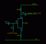
Hi Jan. Of course I would rather think that it is a gain error thing than distortion. Thanks for your observations. Anyway, I think I have found the front end to drive it. TI have a 3 terminal adjustable regulator (what else would I use??) a TL783C that is similar to the LM317 except that it has a mosfet for the series pass element, and has a maximum input to output voltage rating of 125 volts. The other specs are broadly similar to the '317. I got one and quick as a wink I set it up as a x20 voltage amplifier as per the drawing to see how it went.
The gain is set by the ratio of the "collector" resistor to the "emitter" resistor. With a 120vdc supply I could get an undistorted output swing of 100v p/p that would clip symmetrically and have no visible distortion right up to the limit. Frequency response goes out to 50Khz by which time it is slew limiting so if you back off the level a bit the distortion disappears again. If the noise figure is reasonable then I will give this one a try. It was as tame as a little lamb, very nice indeed.
Thanks for your observations. Anyway, I think I have found the front end to drive it. TI have a 3 terminal adjustable regulator (what else would I use??) a TL783C that is similar to the LM317 except that it has a mosfet for the series pass element, and has a maximum input to output voltage rating of 125 volts. The other specs are broadly similar to the '317. I got one and quick as a wink I set it up as a x20 voltage amplifier as per the drawing to see how it went. The gain is set by the ratio of the "collector" resistor to the "emitter" resistor. With a 120vdc supply I could get an undistorted output swing of 100v p/p that would clip symmetrically and have no visible distortion right up to the limit. Frequency response goes out to 50Khz by which time it is slew limiting so if you back off the level a bit the distortion disappears again. If the noise figure is reasonable then I will give this one a try. It was as tame as a little lamb, very nice indeed.
Attachments
From the "Why didn't I think of that?" dept.
Not entirely sure what you mean there Hugh. I need a picture unfortunately. What you did make me think of though is have an npn emitter follower with a current sink load feeding the base of the first transistor. That would also solve my output offset thermal drift problem because as the follower transistor Vbe decreases with temp it pulls up the base of the first PN100 hopefully by the same amount as *it's* Vbe has decreased with temp.
Oh oh.. you mean that cct... I forgot to take my duhh pills today. I actually drew in a 1k simply for illustrative purposes - I think the input impedance of that ic is a lot higher than that. I was driving the thing with a function generator that has a 50 ohm output so this wasn't an issue when I tested it. If the input impedance is high enough I will try a resistive voltage divider from "collector" to "base" to ground to automatically set the "collector" voltage at a stable point rather than have to have a stable bias voltage source. I'm in the middle of building the mother of all multi-rail bench power supplies at the moment so experiments have stopped for a day or so. Back to it very soon.
Not entirely sure what you mean there Hugh. I need a picture unfortunately. What you did make me think of though is have an npn emitter follower with a current sink load feeding the base of the first transistor. That would also solve my output offset thermal drift problem because as the follower transistor Vbe decreases with temp it pulls up the base of the first PN100 hopefully by the same amount as *it's* Vbe has decreased with temp.
Oh oh.. you mean that cct... I forgot to take my duhh pills today.
I actually drew in a 1k simply for illustrative purposes - I think the input impedance of that ic is a lot higher than that. I was driving the thing with a function generator that has a 50 ohm output so this wasn't an issue when I tested it. If the input impedance is high enough I will try a resistive voltage divider from "collector" to "base" to ground to automatically set the "collector" voltage at a stable point rather than have to have a stable bias voltage source. I'm in the middle of building the mother of all multi-rail bench power supplies at the moment so experiments have stopped for a day or so. Back to it very soon.Circlotron,
this looks cool, amps with voltage regulators...
Please can you very briefly explain to me, how it works to make a quasi complementary output stage.
I may be like to use IRFP064 or other N-channels here:
Its not the final circuit yet. Suffering from terrible oszillations...
this looks cool, amps with voltage regulators...
Please can you very briefly explain to me, how it works to make a quasi complementary output stage.
I may be like to use IRFP064 or other N-channels here:
An externally hosted image should be here but it was not working when we last tested it.
Its not the final circuit yet. Suffering from terrible oszillations...
If the output contains distortion and you feed it back to the input...In real life it will be driven from a CD player analog output, so a 20kHz full power sinewave is about as bad as it gets IMHO. Anyone care to offer another opinion there?
More on N-channel FETs only output
Hi,
you may find this page interesting. It is unfortunately in Russian, and the actual diagrams are not very good quality, but missed lines are easily restored. If you have questions, ask me - I may be able to help. You need to go to the page 37 for a complete diagram. This circuit is quite old now (1993-94), but the idea is still interesting. It allows for the same polarity devices in both positive and negative halfs, but it is not quasi-complementary and it is very linear even without the overall NFB. Symmetry is very good and distortion could be as low as 0.05% on 8 ohm load without NFB. It is also very simple.
Cheers,
Al
link: http://anklab.pirit.sibtel.ru/Press/PX/1998/6/index.html
Hi Bernhard. That's a tricky question because you need to have the upper stage the same gain as the lower one. I need to think about it some more.Bernhard said:Please can you very briefly explain to me, how it works to make a quasi complementary output stage. Its not the final circuit yet. Suffering from terrible oszillations...
As for the oscillations, C5 doesnt look good. Put a second resistor in series with R7 and then run C5 to the junction of the two resistors instead of straight to Q1 collector. Same with other three positions. Have the stopper as resistor the only thing connected to the gate.
Re: More on N-channel FETs only output
Thanks.
Hi Al. I downloaded the pic about 2 milliseconds after I read your post, so excited that I was, but the DJVU file format while it is one that IrfanView is supposed to be able to handle, I could not get it to work. Could you or someone else less "graphically challenged" than me dowload it and convert it to to a GIF and put it up here so I can see it? Or is it the one you put here? http://www.diyaudio.com/forums/showthread.php?postid=166853#post166853x-pro said:
Thanks.

Anytime man!
DjVu Browser Plug-in
http://www.lizardtech.com/download/?x=2&p=1&o=1&titl=Download DjVu Browser Plug-in
DjVu Browser Plug-in
http://www.lizardtech.com/download/?x=2&p=1&o=1&titl=Download DjVu Browser Plug-in
- Status
- This old topic is closed. If you want to reopen this topic, contact a moderator using the "Report Post" button.
- Home
- Amplifiers
- Solid State
- Quasi-complementary Hexfet monstrosity.