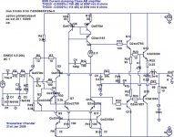
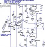
The following topology is an attempt to graft a current-dumping topology around a stock Class-AB Douglas Self Type-II Emitter-Follower Output Stage. While the original idea (Walker and Albinson, 1975) of current dumping was built around a Class-A stage driving a Class-B stage, there's nothing conceptually difficult about using the same idea to correct the non-linearity (crossover distortion, etc.) of a Class-AB stage as well.
The main idea behind this topology is to treat the LTP, VAS and the driver stage as a linear Class-A stage with gain, and the O/P stage as a separate Class-AB voltage-follower. The emitter-to-emitter resistance between the drivers of the Self Type-II stage is split into two equal resistances, and the Class-A output 'corrector current' is obtained from the mid-point of the two. A balanced reactive bridge (a la Quad 405) is driven by a Class-AB voltage-follower driving the low-impedance side of the bridge, and deriving its input from the high-impedance side, which is itself driven by the Class-A combination of the LTP, VAS and driver stages.
In the schematic shown, a standard CFP LTP (Q1-Q2-Q3-Q4) drives a tricked-up VAS pair (Q7-Q10) into a Wilson current mirror (Q6-Q8-Q9). It simulates well with good sonics at all swings, but there's nothing special about the input and VAS stage, and it could be replaced by anything else, including a bootstrapped VAS. The VAS drives a standard Self Type-II driver and output stage, as noted previously, with the Class-A output being derived from the junction of R21-R22, driving one leg of the balanced reactive bridge consisting of R27-L1-R19-C6. The closed-loop gain is set by the ratio (1 + R19/R18). Stability is obtained by a combination of C3-R8, C4-R12 and the bridge capacitance C6.
As shown, it is designed for 80W with a maximum output swing of +/- 36V with +/- 42V rails, but there's no reason why it won't work with different (higher or lower) rail voltages. The quiescent current in the output stage is not critical, and anything from 50 mA to 200 mA should be OK - the simulated value is around 100 mA.
Edit: This concept has been influenced significantly by the very clever work of our Bulgarian friend Widowmaker, with his DoGC and similar current-dumping topologies that he has posted from time to time on this forum.
Attachments
If you remove the balanced bridge (and just retain the feedback gain network, output inductor and Zobel) you'll find that distortion will go up by about 10..20 dB, other things being equal. The contribution of the Class-A stage to the output current is small (~10s of mA at maximum swing), but it plays a crucial role in correcting non-linearity, hence lowering distortion.
Andrew: Yes, more or less. Note that without current-cumping, we'd typically use a higher impedance feedback network than shown. That would in turn affect the compensation schema.
With current dumping, there's a loose constraint on the range of values R19 to attain bridge balance. If it's made too large, C6 will have to be made very small to maintain bridge balance. If C6 gets into the sub-10 pF range, it will be inconvenient to maintain it accurately because of stray capacitances from the tracks. Small values of C6 also adversely affect stability. That constrains it the the range of 10 pF to a few 100 pF, and accordingly constrains R19. We'd also not want to make R19 too small, which would increase its power dissipation substantially. The values shown are about par for the course, and there's some room for fine tweaking to further minimize distortion.
Note that in the schematic shown, just removing R27 not only increases the distortion, but also the character of the distortion, making H3 dominant over H2. If R27 is retained but C6 is removed, the circuit becomes difficult to stabilize. If both R27 and C6 are removed, distortion and instability both increase. Removing R27 and C6 will force changes to both the feedback network as well as compensation schema with recover stability, but distortion will remain higher regardless.
Lumanauw: I played around with Class S for a short while, but found that current-dumping is able to produce produce comparable or lower distortion with much lower circuit complexity. In simulations, I found that the nature of the high-gain Class-A stage employed is critical to maintain stability in Class-S, and not every Class-A stage works well or has good sonics in Class-S. In particular, there is a H3-dominance in most topologies, even when the Class-A stage simulates well on its own. IMHO, current dumping is easier to tweak for good sonics as well as stability.
However, I'll revisit Class-S (or its Technics variant) in simulation eventually - there is scope for reactive bridging there also, which may aid stability and/or distortion.
Glen, why don't you try to understand the Walker and Albinson patent and publications, instead of spouting gibberish? It's fairly simple to verify the LTSpice FFT numbers I posted, and you'll get something similar with a wide variety of BJTs - there's no fancy ultra-linear boutique device required, except for the VAS. You can even substitute the input stage and VAS with something very simple, and you'll still get the 10..20 dB improvement I'm claiming, as compared the version(s) without current dumping.
Edit: With an LME49860 as the Class-A gain stage, and a tricked-up current-dumping Class-A voltage-follower that I'd prefer not to disclose for a few months, I'm already at -160 dB THD20 at 1W into 8 ohms. Even with ordinary diamond buffers as the output stage, you can get to -130..-140 dB without any difficulty. The Class-AB numbers shown are not difficult at all.
Edit: With an LME49860 as the Class-A gain stage, and a tricked-up current-dumping Class-A voltage-follower that I'd prefer not to disclose for a few months, I'm already at -160 dB THD20 at 1W into 8 ohms. Even with ordinary diamond buffers as the output stage, you can get to -130..-140 dB without any difficulty. The Class-AB numbers shown are not difficult at all.
linuxguru said:Glen, why don't you try to understand the Walker and Albinson patent and publications, instead of spouting gibberish? It's fairly simple to verify the LTSpice FFT numbers I posted, and you'll get something similar with a wide variety of BJTs - there's no fancy ultra-linear boutique device required, except for the VAS. You can even substitute the input stage and VAS with something very simple, and you'll still get the 10..20 dB improvement I'm claiming, as compared the version(s) without current dumping.
Edit: With an LME49860 as the Class-A gain stage, and a tricked-up current-dumping Class-A voltage-follower that I'd prefer not to disclose for a few months, I'm already at -160 dB THD20 at 1W into 8 ohms. Even with ordinary diamond buffers as the output stage, you can get to -130..-140 dB without any difficulty. The Class-AB numbers shown are not difficult at all.
LOL!
The answer to my question is obviously “no”.
I didn’t say anything about the validity of the current dumping technique and you can retain the view that I am talking gibberish if you like. I’ll continue to outline the basic lack of understanding of amplifier frequency compensation on your part anyway:
I have “verified” your simulation results, and the problem with your method of obtaining ultra-low THD figures in SPICE is exactly the same as the last time I “verified” that Mullard inspired amplifier you LTspiced and quoted totally unrealistic (in the real world) THD-20 figures for.
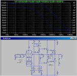
This time the first thing I did was to enter your circuit into LTspice exactly as per the schematic in your opening post, but with the omission of the current dumping network (see attachment).
The output stage was optimally biased with ~50mV emitter-emitter at the output devices (Andy C’s models).
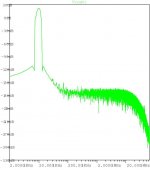
I then ran a transient analysis and THD analysis at 20kHz. THD-20 came in at 0.0013% and, not surprisingly, the amplifier could not even drive (without oscillating) the 10R/100n Zobel network without an isolation inductor.
I then ran a loop gain analysis (see attachment). The unity loop gain frequency is over 6MHz with a phase margin a couple of degrees! There is no way in a million years this circuit will work in real life.
The loop gain at 20kHz is therefore optimistically high and the THD optimistically low.
To return realistic THD-20 figures (which would actually be about 20dB higher) you need to revise the frequency compensation for a unity loop gain frequency at least 6 times lower.
Attachments
Hi, Linuxguru,
Sometime ago I studied this Quad current damping amp. Some difficulties in practice, like : the feedback network resistor gets so low that I need big capacitor value for AC coupling the feedback resistor, the classA stage (predriver Q12-Q13 in your schematic) needs to flow substantial of mA bias current to get the whole thing works properly. This alone make the whole amp quite hot.
Another difficulty is the L construction. It has to be right in all aspect (inner diameter, coil spacing, etc).
 H2 or H3 dominant amps both can sound good.
Sometime ago I studied this Quad current damping amp. Some difficulties in practice, like : the feedback network resistor gets so low that I need big capacitor value for AC coupling the feedback resistor, the classA stage (predriver Q12-Q13 in your schematic) needs to flow substantial of mA bias current to get the whole thing works properly. This alone make the whole amp quite hot.
Another difficulty is the L construction. It has to be right in all aspect (inner diameter, coil spacing, etc).
Don't worry about thisthere is a H3-dominance in most topologies
H2 or H3 dominant amps both can sound good.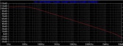
Glen, I've stated fairly clearly that the circuit is difficult to stabilize without the balanced reactive bridge. There's no point in installing C6 alone without balancing all four legs of the bridge. Without R27, but with the remaining 3 legs of the bridge in place (unbalanced), the circuit is stable in simulation with much higher THD20, just as I predicted.
The entire balanced bridge R27-L1-R19-C6 is critical to stability and low distortion - simulation results are fairly meaningless for the current-dumping topology without the entire bridge in place.
When the bridge is balanced, it remains balanced at *all* frequencies. In the s-domain:
sL1 / R19 = R27 * sC6
=> L1/C6 = R19 * R27 and the frequency drops out of the picture. This is critical to the stability of the topology - the bridge is frequency-neutral. C6 is not a lead-compensation capacitor as you understand it, but required to balance the bridge. Calling it a lead compensation capacitor will not necessarily aid your understanding of the topology.
Lumanauw: Yes, the feedback network is relatively low impedance, but it does not appear to hinder biasing or offset matching. The biasing network shown (derived from Widowmaker's earlier postings) does the job just fine. You need an AC coupling cap on the inverting side of a few hundred uF - by no means difficult.
The driver runs hotter than a traditional Class-AB (I have 66 ohms, emitter-to-emitter; traditional Self Type-II drivers tend to have 100-150 ohms), but the current and dissipation are easily manageable with a small heatsink on the drivers. You can also reduce the quiescent driver current by increasing R27 and reducing C6 (to regain balance), but there's a limit to how small C6 can be made without impacting stability. In simulation, C6 can range from 22pF or thereabouts on the low side.
Making a 1% tolerance 2.2 uH inductor is difficult, of course, but you don't need to do that. Just make a very stiff and mechanically stable inductor of approximately 2.2 uH, measure the actual inductance of L1 and capacitance of C6 with a digital LCR meter, and trim the resistive elements of the bridge to obtain balance (this just requires two measured metal-film resistors in series for R19 and/or R27).
The alternative way to balance the bridge is to use a small isolated jig with an audio frequency generator connected to L1-R27 and R19-C6 junctions, and a headphone to L1-R19 and R27-C6 junctions. At bridge balance, the audible signal will null out. It's no more difficult than setting the output stage quiescent current in a conventional Class-AB topology.
http://quad405.com/jaes.pdf
Hi,
The above is plently to chew on as to getting the bridge right /
adding some other components for effective bridge balance.
AFAIU the compensation and stability of a feedforward amplifier
is in no way similar to a standard AB amplifier without the bridge.
In fact AFAICT that is the whole point of feedforward correction.
/sreten.
Hi,
The above is plently to chew on as to getting the bridge right /
adding some other components for effective bridge balance.
AFAIU the compensation and stability of a feedforward amplifier
is in no way similar to a standard AB amplifier without the bridge.
In fact AFAICT that is the whole point of feedforward correction.
/sreten.linuxguru said:Glen, I've stated fairly clearly that the circuit is difficult to stabilize without the balanced reactive bridge. There's no point in installing C6 alone without balancing all four legs of the bridge. Without R27, but with the remaining 3 legs of the bridge in place (unbalanced), the circuit is stable in simulation with much higher THD20, just as I predicted.
I was just interested in simplifying the circuit to see a ‘best possible case’ reduction in the unity loop gain frequency, which was convenient to test as C6 (without the rest of the bridge) is in the common “phase lead” position.
As far as I can ascertain, with the rest of the bridge in place the unity loop gain frequency is still in the vicinity of 5MHz.
Cheers,
Glen
To me this isn't "current dumping" The original concept is that the load is supplied exclusively from a small hi speed class A amp up to the point that the slower outputs can take over. Your circuit seems to show the outputs (and drivers) as supplying the load at all times.
Here's the Class-A current-dumping variant that I referred to in Post #9 above. The power output section is a diamond buffer with tricked-up CFP outputs. This is used as a unity-gain buffer stage for a current-dumping stage, where the inner op-amp (LME49860) is the Class-A gain stage. Distortion is reduced further by wrapping an outer op-amp stage around the whole current-dumping setup (yes, I know I'm cheating by using high-performance op-amps with nested feedback).
The current-dumping bridge consists of (L1 || R2) and R27 on the low-impedance side, and (C8 || R13) and C3 on the high-impedance side. This arrangement lowers the sensitivity to component values and is also easier to stabilize. At bridge balance, there are two independent constraints to be met:
L1 / C3 = R13 * R27 ----------- (1)
L1 / C8 = R13 * R2 ----------- (2)
which are fairly easily satisfied with reasonable values for the components, as shown in the schematic.
This is just an illustrative conceptual schematic - a practical design based on this topology will need additional refinement, particularly in the areas of stability and noise-pickup. It will also run very hot at ~90W dissipation per channel, almost all of which is due to the Class-A output stage quiescent current.
Attachments
- Status
- This old topic is closed. If you want to reopen this topic, contact a moderator using the "Report Post" button.
- Home
- Amplifiers
- Solid State
- Current-dumping Class-AB Self Type-II EF O/P