Hi")
A new amp is on the horizon!
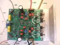
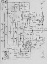
This is an intermediate proto-type PCB for my new amp. This one is 2 plated layers, 2 ounce copper. PCB was drawn using Eagle and made by Advanced Circuits.
I vouch for 'em, good work.
A new amp is on the horizon!
This is an intermediate proto-type PCB for my new amp.
This one is 2 plated layers, 2 ounce copper. PCB was drawn using Eagle and made by Advanced Circuits.I vouch for 'em, good work.
Attachments
Lately I’ve been quite busy doing other things related to life, but I finally found some time over the holidays to invest in a new circuit. I’ve seen a few folks here sharing info about their ultimate amp challenges. I know we all have our own version of the ultimate amp, I find it interesting to see how others have accomplished their “ultimate” status. Hail to those of you who are willing to pis$ into the wind and take a chance that your complex creation might fail.
So…..I’ve been working on an intermediate prototype for my version of the ultimate amp and thought there might be some interest here. This circuit is a culmination of prior circuits, built most definitely as “ugly amps”, but they worked, each better than the last. I didn’t just think this one up overnight. I’m still listening to the ugly amp prior to this build, over 14 months after construction.
  The new one is slightly less ugly, and actually sounds a bit better if it is possible, as far as noise, separation, gain, and power! There are some folks who require an amp made with as few transistors as possible. To each his own I always say. But this project was undertaken with the intention of quality regardless of complexity. As for the play material, if it’s in there, you hear it, clearly. Not all of the bugs are worked out quite yet, it’s very close, and I think it may just in fact work after all.
A little about the circuit……..as you can see, there are a few components involved here. Although at first glance it may appear so, but there are no IC’s in this circuit, it is made completely from discrete components, all analog. I’ve managed to squeeze 179 transistors onto a 4.5” X 5” double sided PCB. This is possible because you don’t need lots of current to amplify a signal in an amplifier circuit until you get to the final stages (unless you use only 5-6 transistors.
  ) You can then choose components that are suitable for a smaller current range. There may be a bunch of 201 size SMD resistors in this circuit, but not one of them has to dissipate more than a few mW, most are in the uW range, not even close their de-rated maximum.
The circuit is actually 8 separate discrete amplifiers, all direct coupled. Everything on the PCB is powered by the high voltage supply. I use a half wave voltage doubler from the main supply, with 470uf caps to supply this power. So the result is +/-24V for high current to source the output transistor channels, and +/- 48V for the rest of the board. This sounds silly, but it really does work without any hum or noise. VERY quiet. All of that circuitry requires only 40mA of current which equates to only about a volt of ripple @ 60Hz. The first 2 amplifiers are the voltage regulators for this supply line, outputs are +/- 42V. Also provides +/- 15V 12mA source. Other than polarity, they are exactly the same circuit. This amplifier simply amplifies a clean DC reference voltage (no Zeners used here , I don’t like Zener voltage references ); the TO-92 with the tab is the series pass device for these 2 amps. The other TO-92’s on this side of the board are the shunt transistors for both polarities.
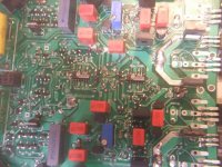
The 3rd amp is the fist gain stage. This amp is a balanced bridge with a cascode VAS, +/-15V. It has 2 functions. 1) Adds voltage gain, for a Av if 20. 2) It provides 2 phases of signal, for a truly balanced output. The sensitivity is so that 0.45Vp will clip the amp. There is a jumper at the input that selects between a balanced or a single end signal input. The circuit uses an “error correction” scheme to make up the difference between currents in the bridge when fed from the single end input source, and creating a balanced output.
The final output transistors’ decoupling caps aren’t in yet, they get in the way of tweaking the other part values….
So…..I’ve been working on an intermediate prototype for my version of the ultimate amp and thought there might be some interest here. This circuit is a culmination of prior circuits, built most definitely as “ugly amps”, but they worked, each better than the last. I didn’t just think this one up overnight.
I’m still listening to the ugly amp prior to this build, over 14 months after construction. The new one is slightly less ugly, and actually sounds a bit better if it is possible, as far as noise, separation, gain, and power! There are some folks who require an amp made with as few transistors as possible. To each his own I always say. But this project was undertaken with the intention of quality regardless of complexity. As for the play material, if it’s in there, you hear it, clearly. Not all of the bugs are worked out quite yet, it’s very close, and I think it may just in fact work after all. A little about the circuit……..as you can see, there are a few components involved here.
Although at first glance it may appear so, but there are no IC’s in this circuit, it is made completely from discrete components, all analog. I’ve managed to squeeze 179 transistors onto a 4.5” X 5” double sided PCB. This is possible because you don’t need lots of current to amplify a signal in an amplifier circuit until you get to the final stages (unless you use only 5-6 transistors. ) You can then choose components that are suitable for a smaller current range. There may be a bunch of 201 size SMD resistors in this circuit, but not one of them has to dissipate more than a few mW, most are in the uW range, not even close their de-rated maximum. The circuit is actually 8 separate discrete amplifiers, all direct coupled. Everything on the PCB is powered by the high voltage supply. I use a half wave voltage doubler from the main supply, with 470uf caps to supply this power. So the result is +/-24V for high current to source the output transistor channels, and +/- 48V for the rest of the board. This sounds silly, but it really does work without any hum or noise. VERY quiet. All of that circuitry requires only 40mA of current which equates to only about a volt of ripple @ 60Hz. The first 2 amplifiers are the voltage regulators for this supply line, outputs are +/- 42V. Also provides +/- 15V 12mA source. Other than polarity, they are exactly the same circuit. This amplifier simply amplifies a clean DC reference voltage (no Zeners used here
, I don’t like Zener voltage references ); the TO-92 with the tab is the series pass device for these 2 amps. The other TO-92’s on this side of the board are the shunt transistors for both polarities. The 3rd amp is the fist gain stage. This amp is a balanced bridge with a cascode VAS, +/-15V. It has 2 functions. 1) Adds voltage gain, for a Av if 20. 2) It provides 2 phases of signal, for a truly balanced output. The sensitivity is so that 0.45Vp will clip the amp. There is a jumper at the input that selects between a balanced or a single end signal input. The circuit uses an “error correction” scheme to make up the difference between currents in the bridge when fed from the single end input source, and creating a balanced output.
The final output transistors’ decoupling caps aren’t in yet, they get in the way of tweaking the other part values….
Attachments
The 4th & 5th amps are the 2 DC servo circuits. These amps measure the final output voltages of each output phase and correct them via the input to 0VDC. This is the only global feedback loop around the entire amplifier, and it’s input is through a low pass filter fc~0.3Hz. There is no global loop for the audio, but rather direct coupled cascade “black box” amplifiers. The DC offset at the speaker terminals of this PCB is 15mV; and 20mV & 35mV each from GND. I still have to experiment with the filter frequencies wrt the input filter and DC servo filter. I may be able to get the “thump” to be rather a smaller sub-sonic signal at turn on. The ugly amp version is tweaked this way so it doesn’t need a relay.
The 6th amp is the VAS. It is also a balanced bridge but a bit different in fb and compensation. It requires a balanced input in order to output a balanced signal with an Av of 4.4. So 20 X 4.4 =88 as a total signal Av. Hey, I can plug up an I-pod and still get almost full power and it would be simple to increase the over-all gain to 100. Each side of this bridge sets the voltage bias for the next two stages….
You can see where I had to run little pieces of green wire at the output gates, I forgot to route in gate Zobel filter caps...…..Doh! It’s all right, a little super glue and it’s just another layer, eh?
The 6th amp is the VAS. It is also a balanced bridge but a bit different in fb and compensation. It requires a balanced input in order to output a balanced signal with an Av of 4.4. So 20 X 4.4 =88 as a total signal Av. Hey, I can plug up an I-pod and still get almost full power and it would be simple to increase the over-all gain to 100. Each side of this bridge sets the voltage bias for the next two stages….
You can see where I had to run little pieces of green wire at the output gates, I forgot to route in gate Zobel filter caps...…..Doh!
It’s all right, a little super glue and it’s just another layer, eh? Attachments
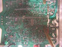
The 7th and 8th amplifiers are also identical. They are the current amplifying followers for each phase output. This circuit produces 28VAC rms output bridged between it and the other output side, so 100W @ 8R, 150W@ 6R with 4 TO-220 (or TO-3P) Hexfets for outputs. I want to do some more testing and maybe build another one (I have 4 more PCB’s) before I try 4R and see how long it takes for the outputs to fail and test the result. I did drop a 38Hz sine wave @ 32Vp across an old 4 Ohm sub-woofer, which bottomed it out, but the signal did not appear to distort on the scope. This was only for a short burst because I didn’t have the bracket mounted to a heat sink and I have neighbors.  IMHO hexfets actually make great audio output transistors, if you use them right. This circuit is a typical HEC hexfet gate driver circuit, but I added a few bells and whistles. A cascode here, a cascode there……
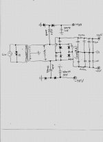
I’ve drawn out what I did. I’m having a problem though. It seems that cross-conduction is a problem with frequencies >100KHz. I’m still trying to figure this one out. I must be missing something, compensation to the error amp maybe? I did notice a little bit of oscillation on the square wave that must be coming from the output circuit.
Sorry ‘bout the hand drawn circuit, but the schematic now only exists as a poster on my wall because I don’t have a 48” computer screen and can’t see the whole thing at once otherwise. I’ve combined a single Vgs multiplier with the HEC, at the expense of a few more volts, so as to get the error amplifiers away from the heat sink and use small signal, faster devices with shorter traces. I finally was able to tune it in so that it tracks with a slight negative T coefficient. I will fiddle with this a bit more too. At start up, the error devices are cold and the bias is a bit high, 300mA. It will settle at about 200mA and may drop to ~100mA when very hot. Anyhow, hexfets need more bias current and I find they are more forgiving when it comes to thermal tracking. Besides, a little extra current when the hardware is cold shouldn’t hurt things, eh? As for damping, well, hexfets have the ability to conduct and inhibit large currents very quickly, if driven to do so.
There is certainly room for improvement here, so any suggestions are most welcome. Other than this minor problem, the rest of the amplifier seems to be working correctly.
Transistor arrays A, D, and G are 'these'. Arrays B & E are 'these' and arrays C & F are 'these'.
The first pre-driver followers for this stage need to be as linear as possible because it is not within any fb loop. The transistor pair I used for these doesn’t seem too popular around here. I can’t imagine why, they are wonderfully linear devices from Toshiba of which I measure Hfe of at least 300 for both polarities. 2SC6026 and 2SA2154. If you look very closely at the output sections, you can see them just in front of the blue pots…. SOT-923 is dang small!!! In this circuit, Ic=4mA, Vce=6V. 24mW, no prob.
I want to do some more testing and maybe build another one (I have 4 more PCB’s) before I try 4R and see how long it takes for the outputs to fail and test the result. I did drop a 38Hz sine wave @ 32Vp across an old 4 Ohm sub-woofer, which bottomed it out, but the signal did not appear to distort on the scope. This was only for a short burst because I didn’t have the bracket mounted to a heat sink and I have neighbors. IMHO hexfets actually make great audio output transistors, if you use them right. This circuit is a typical HEC hexfet gate driver circuit, but I added a few bells and whistles. A cascode here, a cascode there……I’ve drawn out what I did. I’m having a problem though. It seems that cross-conduction is a problem with frequencies >100KHz. I’m still trying to figure this one out. I must be missing something, compensation to the error amp maybe?
I did notice a little bit of oscillation on the square wave that must be coming from the output circuit. Sorry ‘bout the hand drawn circuit, but the schematic now only exists as a poster on my wall because I don’t have a 48” computer screen and can’t see the whole thing at once otherwise. I’ve combined a single Vgs multiplier with the HEC, at the expense of a few more volts
, so as to get the error amplifiers away from the heat sink and use small signal, faster devices with shorter traces. I finally was able to tune it in so that it tracks with a slight negative T coefficient. I will fiddle with this a bit more too. At start up, the error devices are cold and the bias is a bit high, 300mA. It will settle at about 200mA and may drop to ~100mA when very hot. Anyhow, hexfets need more bias current and I find they are more forgiving when it comes to thermal tracking. Besides, a little extra current when the hardware is cold shouldn’t hurt things, eh? As for damping, well, hexfets have the ability to conduct and inhibit large currents very quickly, if driven to do so. There is certainly room for improvement here, so any suggestions are most welcome. Other than this minor problem, the rest of the amplifier seems to be working correctly.
Transistor arrays A, D, and G are 'these'. Arrays B & E are 'these' and arrays C & F are 'these'.
The first pre-driver followers for this stage need to be as linear as possible because it is not within any fb loop. The transistor pair I used for these doesn’t seem too popular around here. I can’t imagine why
, they are wonderfully linear devices from Toshiba of which I measure Hfe of at least 300 for both polarities. 2SC6026 and 2SA2154. If you look very closely at the output sections, you can see them just in front of the blue pots…. SOT-923 is dang small!!! In this circuit, Ic=4mA, Vce=6V. 24mW, no prob.Attachments
- Status
- This old topic is closed. If you want to reopen this topic, contact a moderator using the "Report Post" button.