Not really an AD797 since it's a JFET input amp. Seems stable, sounds good. Sounds close to the original AD797. Maybe a little cleaner than my discrete AD829 clone, but I can't be sure. I'm going to give it some more time.
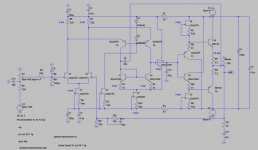
I use Sanyo SA1016 and SC2362, not the Toshibas in the schematic. There are no good models for them. The Sanyos sound more neutral and just as detailed. The perfect small signal transistor.
It's battery powered, 8 x AAA, and pocket sized.
I think it's the floating current mirror that makes it sound different from "AD829", more so than the "magic" transistor or the decompansating capacitor.
Attachments
nelsonvandal said:I think it's the floating current mirror that makes it sound different from "AD829", more so than the "magic" transistor or the decompansating capacitor.
Hi Nelson,
If you are referring "magic transistor" to T1, floating current mirror couldn't exist without one. Have you consider cascading J1/2 with something like 2SK246 alla Borbely? Do you have the same DC operating conditions at input and output of current mirror, could you post few turns of transient analyses from input/output from CM and opamp output?
Nelson: you may want to try moving the base of T1 from the gain node to the output (or a derivative). This will reduce loading on the gain node, and probably give lower distortion as a result. But whether you move the base of T1 or leave it where it is presently at, you probably want to add a bit of level-shifting to give T4 room to operate.
Personally, I would also try feeding C7 from the collector junction of T4/T5 (rather than from the output), and create a local nested feedback loop. IME, stability and RFI immunity frequently go up when you do this.
If you must use resistors RE and RF instead of active current sources, you may want to exchange D1/D2 for a precision voltage reference. The Vf of a normal diode is too easily affected by a variety of factors, and this may result in unwanted current fluctuation (which will degrade the overall performance of the circuit).
You can also improve the distortion of the output stage if you drop the two current sources and instead run a current mirror on either voltage rail, so that the input of the current mirror is fed from the collector of the output device and the output of the current mirror forms the active load for the junction of the drive transistor's emittor and the output transistor's base. To keep the current mirror going, add one of the active current sources that you removed back across the collector of T10 to the collector of T9.
No need for DC offset control?
regards and hth, jonathan carr
Thank you for your suggestions, I'll look in to them and run some simulations. I'm somewhat limited because of board layout and available space, but I'll take the experience and your input with me to forthcoming projects.
Could you please explain what level shifting is and how I could implement it. I'm not so clever.
What voltage reference could be used instead of the two diodes? In one amp I use a 4.7 V zener, and that amp sounds better, but then it can't be run effectivly on batteries because of the reduced voltage swing. I couldn't find a 1.2 V Zener.
The DC is in the need of some trimming by paralleling R1 or R2, but the offset is "only" 20 - 30 mA untrimmed. All transistors except the output pair are closely matched. I'm done using pot's for offset trimming because of high price, board space and noise (I don't think the ones I've bought at ELFA from BI Technologies are of good quality).
The amp runs perfectly well without the transistor T1, but sounds better with it. I did the mods from AD829 to AD797 in stages - 1. the floating CM 2. the decomp cap 3. transistor T1.
DC at collector of T5 is 38 mV and of T6 is 22 mV, almost exactly the same as simulated. Is that a problem?
Yes I've considered cascoding the input pair. I have a couple of SK246 for future experimenting. My favourite though is CFP input with JFET/bipolar. It does wonders to the sound, more than any other tweak. I suppose both CFP and cascoding à la Lavardin/peufeu is even better. My next amp will definately use CFP input.
Hi Jonathan
Glad to see you
Glad to see you
Happy Holidays!Still alive and active
dimitri said:Are these disto graphs measured or simulated?
They are simulated. I have no means of measureign the real thing exsept by a DMM and my pair of ears.
nelson:
Some more things I noticed after taking a closer look at your circuit (unless my eyes are deceiving me - grin).
If you are actually feeding 2mA each through Re and RF plus 3mA more via T1 (7mA), the math doesn't add up with a current consumption of 4mA through J3 plus 5mA through J7 (9mA). And if you also consider that IRE + IRF are feeding 4mA but the current consumption of IJ3 is likewise 4mA, your folded cascodes are going to be sitting outside in the street with a hat in front of them, begging for someone to give them some current (^o^).
IOW, there may be discrepancies between the real behaviour of the circuit and your present simulations. You should probably try to sort out the basic arithmatic of the circuit before taking what the simulations say too literally.
Level shifting means to introduce a voltage offset, in this case so that more voltage is maintained across the series connection of R2-T4 (say 1.5V). How much voltage do you measure across the series connection of R2-T4 in the real circuit?
For a low-value voltage reference, you could try National Semiconductor's LM4051. It comes in 1.225V & adjustable versions, and has a SOT23 package.
Dimitri: You are right. It has been years, hasn't it. My workload grew to the point where I could no longer afford the time for much internet posting or email stuff. Hopefully, now, I can keep everything more under control. Have to be careful of writing too-lengthy posts (heh, heh).
I hope that you are doing well!
happy holidays, jonathan carr
Some more things I noticed after taking a closer look at your circuit (unless my eyes are deceiving me - grin).
If you are actually feeding 2mA each through Re and RF plus 3mA more via T1 (7mA), the math doesn't add up with a current consumption of 4mA through J3 plus 5mA through J7 (9mA). And if you also consider that IRE + IRF are feeding 4mA but the current consumption of IJ3 is likewise 4mA, your folded cascodes are going to be sitting outside in the street with a hat in front of them, begging for someone to give them some current (^o^).
IOW, there may be discrepancies between the real behaviour of the circuit and your present simulations. You should probably try to sort out the basic arithmatic of the circuit before taking what the simulations say too literally.
Level shifting means to introduce a voltage offset, in this case so that more voltage is maintained across the series connection of R2-T4 (say 1.5V). How much voltage do you measure across the series connection of R2-T4 in the real circuit?
For a low-value voltage reference, you could try National Semiconductor's LM4051. It comes in 1.225V & adjustable versions, and has a SOT23 package.
dimitri said:Hi Jonathan
Glad to see you
Happy Holidays!
Dimitri: You are right. It has been years, hasn't it. My workload grew to the point where I could no longer afford the time for much internet posting or email stuff. Hopefully, now, I can keep everything more under control. Have to be careful of writing too-lengthy posts (heh, heh).
I hope that you are doing well!
happy holidays, jonathan carr
Oh, I'm sorry! It was a slip of thoughts. It's the value from "AD829". The current through J3 is 2 mA, not 4 mA.jcarr said:nelson:
Some more things I noticed after taking a closer look at your circuit (unless my eyes are deceiving me - grin).
If you are actually feeding 2mA each through Re and RF plus 3mA more via T1 (7mA), the math doesn't add up with a current consumption of 4mA through J3 plus 5mA through J7 (9mA). And if you also consider that IRE + IRF are feeding 4mA but the current consumption of IJ3 is likewise 4mA, your folded cascodes are going to be sitting outside in the street with a hat in front of them, begging for someone to give them some current (^o^).
It seems that T1 take whatever current's left. If I increase the current sunk by J7, all that happens is an increase in current through T1.
From a DC perspective, LTSpice almost always predict the real circuit. Some changes have to be made because of varying specs of the transistors.jcarr said:
IOW, there may be discrepancies between the real behaviour of the circuit and your present simulations. You should probably try to sort out the basic arithmatic of the circuit before taking what the simulations say too literally.
667 mV. The voltage over the resistor is 35 mV, so the current is a little low. I can increase the current through the cascodes by lowering the RE/RF to 270R. I want 1 mA through them.jcarr said:
Level shifting means to introduce a voltage offset, in this case so that more voltage is maintained across the series connection of R2-T4 (say 1.5V). How much voltage do you measure across the series connection of R2-T4 in the real circuit?
Thank you. I'll see if I can find one. ELFA doesn't stock them. Could TS431 be used?jcarr said:
For a low-value voltage reference, you could try National Semiconductor's LM4051. It comes in 1.225V & adjustable versions, and has a SOT23 package.
I'll keep my eyes open for your posts.jcarr said:
Dimitri: You are right. It has been years, hasn't it. My workload grew to the point where I could no longer afford the time for much internet posting or email stuff. Hopefully, now, I can keep everything more under control. Have to be careful of writing too-lengthy posts (heh, heh).
I hope that you are doing well!
happy holidays, jonathan carr
Hi Nelson,
Instead T1 try darlington connected 2 npn, 1st one with 5k emitter resistor, 2nd one with 39R, then connect 3rd one npn on top on 2nd (cascode), base of 3rd connect at opamp output. That will give you level shifting for more voltage over R2-T4 and less loading at CM output. Adjust RG1 to have ~0DCV at input/output of CM as well as opamp output. You could use simple Vbe multiplier for D1/2 to get ~1V25, try 1k for both resistor and 1 npn.
Instead T1 try darlington connected 2 npn, 1st one with 5k emitter resistor, 2nd one with 39R, then connect 3rd one npn on top on 2nd (cascode), base of 3rd connect at opamp output. That will give you level shifting for more voltage over R2-T4 and less loading at CM output. Adjust RG1 to have ~0DCV at input/output of CM as well as opamp output. You could use simple Vbe multiplier for D1/2 to get ~1V25, try 1k for both resistor and 1 npn.
nelsonvandal said:The current through J3 is 2 mA, not 4 mA.
OK, so you have 1mA each running through J1/J2/T5/T6. Should be OK. However, with the signal-defining elements each running at 1mA, 3mA for T1 seems a little odd. I'd either get T1 also down to 1mA (by reducing J7 to 3mA) with the goal of reducing power consumption and helping battery life, or raise everything to maybe 2mA.
It seems that T1 take whatever current's left. If I increase the current sunk by J7, all that happens is an increase in current through T1.
This is true for nearly any kind of shunt regulator (which is what T1 is functioning as). The shunt element (T1) eats up whatever current is left over, and in so doing cancels out the differences and fluctuations in current. It isn't like T1 has a fixed operating current, nor should it.
667 mV. The voltage over the resistor is 35 mV, so the current is a little low.
That is low, especially considering the variable transistor parameters that you get with non-monolithic semiconductor processs. I think you may get better and more consistent/stable performance if you add a little voltage shift to either the base or emitter of T1.
I'll see if I can find one. ELFA doesn't stock them. Could TS431 be used?
Apart from losing some voltage headroom due to the difference between the 2.5V Vref of a 431 as opposed to the 1.225V Vref of a LM4051, I don't think there should be much problem.
regards & hth, jonathan carr
Hi,
could D1+D2 be replaced with a red LED? I have 1.55V @ 2mA and some are even lower.
Do the output followers need as much as 30mA of bias? Particularly if powered by battery.
Is it worth cascoding the J3 & J4 CCSs?
What about adding a diode connected sot23 transistor to the emitter of T1? However, the offsets on either side of the mirror are only 38mV & 22mV. That's just 16mV of unbalance across the mirror.
Is it worth adding some real capacitor and trace parameters to the theoretically perfect decoupling shown in the sim?
And my final question: what changes, if any, to allow an increase of supply voltage to +-20Vdc? CFP the input as Nelson has suggested?
Jonathan,
TS431IZ is specified to be adjustable between 1.24 and 6 V, so I think it could be used. It's a bit expensive, but hell this hobby's not cheap anyway. https://www1.elfa.se/data1/wwwroot/webroot/Z_DATA/07305345.pdf
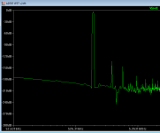
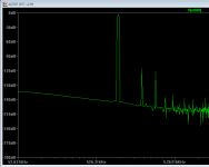
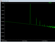
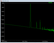
The picture below shows why I choose 3 mA through T1. When it's "starved" to 1 mA, I get this nasty dip in sim. At higher swing it looks even nastier.
Andrew,
I've tried red LEDs, but I didn't find it improved anything unless two were used in series with decreased voltage swing as a result.
I've tried cascoding J3 with an SK246, and I couldn't hear any difference.
I've not run it with more than +/- 9 V, but with with the extra swing a 4.7 V zener and some larger emitter resistors on the CM can be used. It sounds better this way. At least does the AD829 clone. I haven't tried it on this AD797 clone.
I could add a diode to the emitter of the T1 without any hassle and see what it does.
30 mA is kind of arbitrary, to have some margins driving headphones. Since I use HD650 I could have settled for half and still have some margins. The playing time with 950 mAh batteries is still OK.
aparatusonitus,
I'm going to run some sims with a Vbe multiplier and maybe do some listening tests tomorrow. I've seen your AD797-clone. Did you ever build it? What did it sound like?
This amp sounds very good. Very neutral. For the first time since I can't remember when I really have a hard time to "hear" the amp. The sound is warm without being obviously colored. The monolithic AD797 is a little drier and brighter. It's cleaner yet more enjoyable than the AD829 clone. I don't care about higher OLG and distortion towards the odd spectrum and such, when it sounds good.
TS431IZ is specified to be adjustable between 1.24 and 6 V, so I think it could be used. It's a bit expensive, but hell this hobby's not cheap anyway. https://www1.elfa.se/data1/wwwroot/webroot/Z_DATA/07305345.pdf
The picture below shows why I choose 3 mA through T1. When it's "starved" to 1 mA, I get this nasty dip in sim. At higher swing it looks even nastier.
Andrew,
I've tried red LEDs, but I didn't find it improved anything unless two were used in series with decreased voltage swing as a result.
I've tried cascoding J3 with an SK246, and I couldn't hear any difference.
I've not run it with more than +/- 9 V, but with with the extra swing a 4.7 V zener and some larger emitter resistors on the CM can be used. It sounds better this way. At least does the AD829 clone. I haven't tried it on this AD797 clone.
I could add a diode to the emitter of the T1 without any hassle and see what it does.
30 mA is kind of arbitrary, to have some margins driving headphones. Since I use HD650 I could have settled for half and still have some margins. The playing time with 950 mAh batteries is still OK.
aparatusonitus,
I'm going to run some sims with a Vbe multiplier and maybe do some listening tests tomorrow. I've seen your AD797-clone. Did you ever build it? What did it sound like?
This amp sounds very good. Very neutral. For the first time since I can't remember when I really have a hard time to "hear" the amp. The sound is warm without being obviously colored. The monolithic AD797 is a little drier and brighter. It's cleaner yet more enjoyable than the AD829 clone. I don't care about higher OLG and distortion towards the odd spectrum and such, when it sounds good.
Attachments
Nelson,
the full schematic I have of the AD797 is similar to what you have drawn but differs a bit.
I would add cascoding of the input stage JFETs.
I would also try some other BJTs for the output stage. Sanyo has some very good medium current BJTs that you might want to try.
Happy New Year!
Sigurd
the full schematic I have of the AD797 is similar to what you have drawn but differs a bit.
I would add cascoding of the input stage JFETs.
I would also try some other BJTs for the output stage. Sanyo has some very good medium current BJTs that you might want to try.
Happy New Year!
Sigurd
Jonathan -
it is very nice to see you here again!
It has been a while.....
Sigurd
it is very nice to see you here again!
It has been a while.....
Sigurd
jcarr said:
OK, so you have 1mA each running through J1/J2/T5/T6. Should be OK. However, with the signal-defining elements each running at 1mA, 3mA for T1 seems a little odd. I'd either get T1 also down to 1mA (by reducing J7 to 3mA) with the goal of reducing power consumption and helping battery life, or raise everything to maybe 2mA.
This is true for nearly any kind of shunt regulator (which is what T1 is functioning as). The shunt element (T1) eats up whatever current is left over, and in so doing cancels out the differences and fluctuations in current. It isn't like T1 has a fixed operating current, nor should it.
That is low, especially considering the variable transistor parameters that you get with non-monolithic semiconductor processs. I think you may get better and more consistent/stable performance if you add a little voltage shift to either the base or emitter of T1.
Apart from losing some voltage headroom due to the difference between the 2.5V Vref of a 431 as opposed to the 1.225V Vref of a LM4051, I don't think there should be much problem.
regards & hth, jonathan carr
Sigurd Ruschkow said:Sanyo has some very good medium current BJTs that you might want to try.
The Sanyos look good on paper, and they also work well if you don't push much current through them, but when you do want more current, my experience has been that the Toshiba 2SA1837/2SC4793 complementary pair tend to do better (although I am not so fond of fully-insulated TO-220s in general - too easy to crack the plastic when tightening them against a metal heatsink).
Jonathan - it is very nice to see you here again! It has been a while.....
Sigurd! Likewise, a pleasure to talk to you again.
Hopefully now I will be able to strike a better balance between work and posting and communications than in the past.
Hope you have a great New Year
- Status
- This old topic is closed. If you want to reopen this topic, contact a moderator using the "Report Post" button.
- Home
- Amplifiers
- Solid State
- Discrete AD797 up and running