Maybe something like this would be a good starting proposal.
")
An externally hosted image should be here but it was not working when we last tested it.
Ingenius circuit! Haven't seen that. Possible drawback: the output cannot swing close to the rail as there is no possibility to feed the mosfet with a higher supply voltage, and there are two Re's in series which also limits output level with high currents. You'll need a higher supply voltage than usual for a specific output.
Other than that, why not try it. You probably can tack it onto a 'normal' Vas driver.
Jan Didden
Other than that, why not try it. You probably can tack it onto a 'normal' Vas driver.
Jan Didden
Well Jan, first thanks, than some explanations.
Output rails are +/- 50V and are separate from supply rails of voltage amplifier; these can be arbitrary from +/- 55V up.
Two resistors valued 22ohms flows driver current and therefore are not influential to output current nor limits it.
I have to remind you that MOS-FET's are drivers here.
Output rails are +/- 50V and are separate from supply rails of voltage amplifier; these can be arbitrary from +/- 55V up.
Two resistors valued 22ohms flows driver current and therefore are not influential to output current nor limits it.
I have to remind you that MOS-FET's are drivers here.
A potential problem I see - the NPN:s and PNP:s might not share current that well under all conditions. This is because they are driven with about the same current but current gains can be all over the place. Maybe beta-droop comes to your rescue though.
Doesn't Bryston use something similar but with BJT drivers?
Doesn't Bryston use something similar but with BJT drivers?
What we are talking about here is new version of Insulated Gate Bipolar Transistor or IGBT semiconductor in balanced configuration (BIGBT).
Implementations of BIGBT device are versatile and can be used in output stages of different kind of power devices.
Current devided among NPN/PNP devices is similar like in parallel configuration, the transistors have to have similar-equal Hfe. MOS-FET driver is symmetricaly loaded with one BE current per output pair.
In audio:
What you gain is voltage driven powerful output device which can be easily managed by VAS stage. That means you need less stages and shorter signal path is guaranteed. Also you gain positive performance of both kind of output configuration: common emitter and common collector follower.
Bryston
Bryston makes some amplifiers with similar 'compound' output transistors. But they only use BJTs.
See e.g. the Bryston 3B-SST
http://bryston.com/BrystonSite05/BrystonDocs.html
Steven
Bryston makes some amplifiers with similar 'compound' output transistors. But they only use BJTs.
See e.g. the Bryston 3B-SST
http://bryston.com/BrystonSite05/BrystonDocs.html
Steven
Lazy Cat,
Very mind-tickling circuit indeed, I love it when experimenters post their ideas for others to see!
A question for you and for all:
If you have both a common emitter BJT AND a common collector BJT as the output devices (they are in parallel), then can your output stage have a voltage gain greater than 1?
Hi Lazy CatLazy Cat said:... It's my favourite output stage by far and believe me I tried them all.
How linear is your IGBT output stage?
Re: Bryston
If you want to loose all the beauty and synergy of BIGBT symmetry than of course you can use BJT as well.
But I have to remind you of one major drawback in the case of using BJT instead of MOS-FET - you loose symmetry on driving NPN/PNP output transistors. Output transistor at driver's emitter end would be forced extencialy by driver BE current influence. That unsymmetry causes all kind of problems in DC and AC conditions and it's audible too.
In amplifier design we want to achieve the kind of synergy that many perfect separate stages act as one. And that one good single stage in our case output stage, has to be unvisible for previous stage, like constant impedance load, resistor. If you look at post #2, voltage amplifier senses app. 11 kohms and few pF to ground at all power conditions with no extra currents. Almost perfect I think.
Steven said:Bryston makes some amplifiers with similar 'compound' output transistors. But they only use BJTs.
If you want to loose all the beauty and synergy of BIGBT symmetry than of course you can use BJT as well.
But I have to remind you of one major drawback in the case of using BJT instead of MOS-FET - you loose symmetry on driving NPN/PNP output transistors. Output transistor at driver's emitter end would be forced extencialy by driver BE current influence. That unsymmetry causes all kind of problems in DC and AC conditions and it's audible too.
In amplifier design we want to achieve the kind of synergy that many perfect separate stages act as one. And that one good single stage in our case output stage, has to be unvisible for previous stage, like constant impedance load, resistor. If you look at post #2, voltage amplifier senses app. 11 kohms and few pF to ground at all power conditions with no extra currents. Almost perfect I think.
rtarbell said:Lazy Cat,
Very mind-tickling circuit indeed, I love it when experimenters post their ideas for others to see!
A question for you and for all:
If you have both a common emitter BJT AND a common collector BJT as the output devices (they are in parallel), then can your output stage have a voltage gain greater than 1?
In the case of post #2 voltage gain is 1, but there are many ways to raise voltage gain of the output stage; resistors divider at the right position can do it. But seriously, leave the voltage gain to VAS.
boraomega said:Izvrsno! Vrlo duhovita ideja! Je li to probano u praksi?
Translation: "Excellent! Very ingenious idea! Is it tested in practice?"
Thanks. Yeeesssss ....
KLe said:
Hi Lazy Cat
How linear is your IGBT output stage?
As linear as you want it to be.
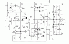
Boraomega, nice and sophisticated VAS, two cascoded diferential stages with intermediate Q5,Q27 gain transistors. I like it.
Good position of high freq compensation filtering, particularly 220ohm/220pF, also there are necessarily R15, R16. I think there's not much to add.
In sense of your concept here maybe you can replace R10, R11 with current mirrors and use DC servo instead of C7 and maybe some AC filtering from anode D1 to ground.
Oh, I almost missed one very important thing, you must put 22k VAS load resistors from collectors Q18, Q21 to ground for better linearity and stability. Otherwise VAS has no proper load in sense of output stage.
- Status
- This old topic is closed. If you want to reopen this topic, contact a moderator using the "Report Post" button.
- Home
- Amplifiers
- Solid State
- Balanced IGBT for amplifier output