The circuit around Q8 and Q11 has pretty undefined behaviour. Better would be to remove Q8 and Q11 and put biasing between bases of Q7 and Q10.
Unless Q8, Q11 is saturated or driven in reverse there is no way for the signal to get to the output right now. (Input is to the collector???)
Unless Q8, Q11 is saturated or driven in reverse there is no way for the signal to get to the output right now. (Input is to the collector???)

Perhaps you should go back and read my explanation of how the circuit works. If you are still having a problem understanding how it works I will try to address your concerns. This is not a simulated circuit only. At least 200 have been built and tested. It does work in spite of simulations.megajocke said:The circuit around Q8 and Q11 has pretty undefined behaviour. Better would be to remove Q8 and Q11 and put biasing between bases of Q7 and Q10.
Unless Q8, Q11 is saturated or driven in reverse there is no way for the signal to get to the output right now. (Input is to the collector???)
Re: Well Steve... seems to me you will give us a nice Christmas gift
You must have received the E-mail from c2cthomas. He has been very busy lately and is only now getting around to picking up the parts from me to send to you.
destroyer X said:
I thank you very much for that.
regards,
Carlos
You must have received the E-mail from c2cthomas. He has been very busy lately and is only now getting around to picking up the parts from me to send to you.
Re: Very interesting unit.... was nice into the simulator
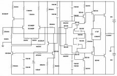
I placed C6 in the wrong place again. Corrected schematic is attached.
The 56K resistor you have drawn parallel to C6 is not in my schematic. The 56K in that area is parallel with the diodes as you have shown. It appears you have an extra R.
Carlos:destroyer X said:Yes.....not needed that resistance between driver's emitters.
regards,
Carlos
I placed C6 in the wrong place again. Corrected schematic is attached.
The 56K resistor you have drawn parallel to C6 is not in my schematic. The 56K in that area is parallel with the diodes as you have shown. It appears you have an extra R.
Attachments
I didn't say it doesn't work, just that its behaviour is a bit undefined!Steve Dunlap said:
Perhaps you should go back and read my explanation of how the circuit works. If you are still having a problem understanding how it works I will try to address your concerns. This is not a simulated circuit only. At least 200 have been built and tested. It does work in spite of simulations.
I had a look at it again, what happens is the one with higher gain (the NPN in the posted simulation) saturates and the other transistor will regulate bias. So it will work.
The problem is that when Q13 draws base current the current through Q8 decreases, making that transistor saturate (if there isn't a big difference in hfe between Q8 and Q11) instead of Q11. This will cause the input voltage needed for the same output voltage to be higher which will cause unneccesary crossover distortion when some non-zero but undefined output current value is crossed.
A simple fix would be a short from C-E over one of Q11 or Q8. The transistor could then be replaced by a diode if one wants. Or just use transistors with very unmatched current gains

I feel you still do not understand what is going on here. There is nothing undefined (to me anyway) about the way this works. Try following the signal from the base junction of Q7 and Q10 through to the outputs.
Your "simple fix" may work in a simulation but if you try this on a working unit I'm afraid you will let all the smoke out.
Your "simple fix" may work in a simulation but if you try this on a working unit I'm afraid you will let all the smoke out.
Why did Q8 just swap its E and C in your new schematic?
But if that is the way it's built then it's likely to work just fine due to the poor hfe of transistors working in reverse.
If I trace the signal in the old schematic from their base junction I find the signal at Q7 and Q10 emitters with a bit of bias voltage. Then this goes to the collectors of Q8 and Q11. Can't get any further unless one or both of them is saturated or they are driven in reverse. One will be saturated because:
Q9, Q12 is pulling their emitters apart. This will cause current to flow through the diode string turning the transistors on. The transistors will turn on so that voltage between Q9, Q12 collectors becomes the drop over diode string + their own vbe voltage. Ok?
Potential at Q7, Q10 emitters will be between Q9, Q12 collector potential. This means Q8 and Q11 is working in the forward mode. The current through the bias string will be so that both Q8 and Q11 conduct. This means it will be determined by the one with highest Ic/Beta quotient. That transistor will saturate.
Why are you talking about simulation? It's pretty obvious without simulating the circuit that it's going to work that way. And besides, if none of Q8, Q11 were saturated then you would be driving the signal into their high impedance collectors, unable to excert any control over their emitter current and output voltage of the stage.
Or the faster explanation: Two transistors are in series. They have the same collector current and same base current. What will happen? The one with higher current gain saturates. That is pretty obvious.
In the case where output signal is drawn:
Two transistors have the same base current.
Collector current is different, we can assume same current gain for simpleness sake.
Both transistors are conducting.
This means Ib >= max(Ic1, Ic2)/beta which means the transistor with the lower collector current will be saturated, and maybe the other one too if needed to try bring their emitters together (but won't happen in this circuit). Inses lätt.
And this leads to a deadband at some current.
Thank you very much, another Christimas gift to me
I am feeling great because of that.
Yes, i have perceived my wrong resistor into the driver's emitter... i see not needed... two base to emitter junctions in series and the capacitor will hold the AC signal as a resistance.
Jenning is in contact...also he has Duda's adress for boards delivery and some small parts.
Schematic received, after use to assemble will be burned..will not be into my computer hard drive.
Will not show schematic, not allow people to see, to copy, no pictures with details, will not allow the equipment to be borrowed as people may try to copy, will not sell, will not publish, will not tell secrets and details.... i will also build the one published into the thread to listen to it too (simplified version)
Beginning of next year those boards will be into my hands... Duda is someone to trust..he will not even open the envelope as he never do such kind of things... high quality friend, decent guy.
No one will have copy of your schematic, even my dear friend Hugh will not have...the same procedure he asked to me...not to show will be now applied to himself.
A hell when we create rules.... because we have to obbey them.
I have parts Steve... if you think there are critical parts (I believe you think alike i think..transistors are transistors only, without big magic..have gain, noise, polarity, operational frequency and better operation point related biasing and colector to emitter voltage) then send me the critical ones... the op amp if needed and boards only is what i really need..in the reality one channel is enougth to me as i have not a good room to listen a perfect stereo..not a prepared room with correct dimensions and analised about reflections and absortions..also i have not a reference speaker..so... stereo is not a real need... it is interesting but not too much.
Also sound stage depends on blending, on capacitors and in special into the supply (double supply and electronic filtering into the higher voltage earlier stages)...so.... having some care we can "arrange" the sound stage we want using those procedures.
regards,
Carlos
Why did Q8 just swap its E and C in your new schematic?
Because I drew it incorrectly. The corrected schematic is attached. Thank you for catching that.
If I trace the signal in the old schematic from their base junction I find the signal at Q7 and Q10 emitters with a bit of bias voltage. Then this goes to the collectors of Q8 and Q11. Can't get any further unless one or both of them is saturated or they are driven in reverse.
The voltage between the emitters of Q7 and Q10 is 1.2V Both transistors are on and conducting. If the voltage at the base of Q7 goes high then the emitter will go high also. When the emitter of Q7 goes high then the emitter of Q8 goes high. The current form the current source Q9 is now divided between the emitter of Q8 and the base of Q13. Less current flows in the emitter of Q8 and as a result, less current flows in the base. The base currents for Q8 and Q11 are always equal but not always constant. When the base current is reduced in Q11 (because it is reduced in Q7) then Q11 begins to turn off thus increase it's resistance and as a result, increasing the voltage on the base of Q16 keeping it turned on. The same basic thing happens in reverse for a negative going input.
Attachments
To Megajocke :
Yes! Someone is seeing these "cascoding" transistors like me : they logically are working in saturated mode because Vce is to small, so they behave like a small value resistor, modulated by the Ib value to a small extent! Actually tghis analysis was valid when there was only 2 diodes in the "polarisation" circuit (original post), now there is 3 so it should be much closer from the elbow of the curve toward standard transistor effect.
I would still want the Microcap file if someone has a good one...
In my Microcap file, I get awfull crossover distortion...
There must be something wrong...
Regards
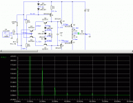
juma said:Hi Steve,
I made a sim in CircuitMaker2000 and voltage values correspond pretty good to those given in your schematic.
I attach a pic of simulated FFT of your output stage with 25V/10Khz input - does it look like a real-life circuit result ?
Thanks
That is a pretty good result. I don't think I have ever done quite that well in a real unit. I see you found that offensive 7th harmonic that someone thought would ruin the sound.

darian said:To Megajocke :
Yes! Someone is seeing these "cascoding" transistors like me : they logically are working in saturated mode because Vce is to small, so they behave like a small value resistor, modulated by the Ib value to a small extent! Actually tghis analysis was valid when there was only 2 diodes in the "polarisation" circuit (original post), now there is 3 so it should be much closer from the elbow of the curve toward standard transistor effect.
I would still want the Microcap file if someone has a good one...
In my Microcap file, I get awfull crossover distortion...
There must be something wrong...
Regards
The number of diodes in the series does not change the current flowing, only the voltage difference between the bases and therefore the emitters. I am not sure what you mean by "polarisation". The diodes with the resistor parallel to two of them simply sets the voltage drop, which of course varies with the base current.
I also do not understand why you refer to the "cascoding" transistors. The voltage and current varies on all three pins so I do not consider this a cascode arrangement.
The distortion in a real unit measures fairly low. I cannot say why your simulation shows it to be high.
Steve Dunlap said:
The voltage between the emitters of Q7 and Q10 is 1.2V Both transistors are on and conducting. If the voltage at the base of Q7 goes high then the emitter will go high also. When the emitter of Q7 goes high then the emitter of Q8 goes high. The current form the current source Q9 is now divided between the emitter of Q8 and the base of Q13. Less current flows in the emitter of Q8 and as a result, less current flows in the base. The base currents for Q8 and Q11 are always equal but not always constant. When the base current is reduced in Q11 (because it is reduced in Q7) then Q11 begins to turn off thus increase it's resistance and as a result, increasing the voltage on the base of Q16 keeping it turned on. The same basic thing happens in reverse for a negative going input.
Yes, that's right. But the "When the emitter of Q7 goes high then the emitter of Q8 goes high." part is the part which only is true if Q8 and/or Q11 is saturated. Otherwise they will work as cascodes isolating the output stage from the input signal. Now, one of the will always be saturated due to circuit conditions but if their current gains are about the same then there will be a deadband at some output current because the transistor on the other side saturates instead.
If you look at the node potentials in your own simulations you can see that the NPN is saturated in the quiescent state, just as expected.
darian said:To Megajocke :
Yes! Someone is seeing these "cascoding" transistors like me : they logically are working in saturated mode because Vce is to small, so they behave like a small value resistor, modulated by the Ib value to a small extent! Actually tghis analysis was valid when there was only 2 diodes in the "polarisation" circuit (original post), now there is 3 so it should be much closer from the elbow of the curve toward standard transistor effect.
I would still want the Microcap file if someone has a good one...
In my Microcap file, I get awfull crossover distortion...
There must be something wrong...
Regards
I'd expect it to have awful crossover distortion, but not neccesarily at zero output current. What happens if you unbalance the current gains of the transistors on each end of the diode stack? It should move the deadband to another output current.
Shorting E-C on one of those two transistors should remove the deadband distortion.
- Status
- This old topic is closed. If you want to reopen this topic, contact a moderator using the "Report Post" button.
- Home
- Amplifiers
- Solid State
- Krill - The little amp that might...