Citation 13
I posted something about that amp, search for "Citation 13". Amazing that no one has built it? Do people do some "DIY" nowadays? Anyway, I've built it. Used IRF540's and amp sounds very good. PCB - don't have any drawings, did it by hand, straight onto board. If you build it, please let us know how do you like it.
Jack
Hi!
Please check this thread here for more info on Citation 12.
http://www.diyaudio.com/forums/showthread.php?s=&threadid=5843&perpage=10&highlight=&pagenumber=1
BTW I made one using IRFP250N long time back. Here is PCB layout for the same. Only extra additions were .47E resistors in Source and drain of O/P devices.
Regards
Rahul
Track layout attached
Attachments
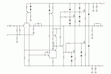
Hi Diyaudio Members,
I just wondering if the Citation would work as higher power amp, for example 200W/4ohm.
Is the driving method of the output devices causing any problem, such as asymmetry?
Thanks, best regards,
PS.: A schema attached. Only take the output stage into account, don't care about the small signal part of the schema.
Attachments
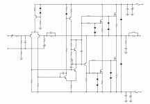
The diodes from the gates of the MOSFETs to the +V rail are not necessary in your modification, they were included in the original to produce symetrical clipping, because the original's bootstrapped VAS can swing above the +V rail. The diodes limit the swing to the +V rail. In your case, the differential + current mirror VAS cannot swing over the supply rail so the diodes are not necessary.
Ilimzn,
Thanks for your clear comment, schema updated.
Regards,
PS.: Anyway, what do you think,
Thanks for your clear comment, schema updated.
Regards,
PS.: Anyway, what do you think,
Is the driving method of the output devices causing any problem, such as asymmetry?
Attachments
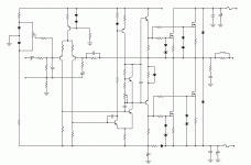
edl said:Ilimzn,
Thanks for your clear comment, schema updated.
PS.: Anyway, what do you think:
Is the driving method of the output devices causing any problem, such as asymmetry?
The answer to that question is clearly yes - but with this kind of corcuit it is unavoidable. You can just attempt to minimize it. For one, the top MOSFET's gate is driven by a current source, the bottom by a current source in parallel with a resistor. As a result, the top MOSFET gate can be both charged and discharged equally, while the bottom one is not. With properly chosen standing current for the driver transistor of the bottom MOSFETs, this should not be a major problem, but it should still be stressed that the circuit is funadamentally asymetrical.
Your second updated schematic has a problem - it is ESSENTIAL that the resistor between gates of the lower MOSFETs and -V rail is connected to the source side of the voltage rail, because this resistor develops the gate to source voltage. In your schematic, additional voltage is developed across the diode and resistor. Since there is a capacitor on the other side of these, initially, when the cap is charging up, the additional voltage will turn the lower MOSFETs fully on resulting in a LARGE full output thump (goodbye speakers and possibly MOSFETs), and even if you forget about that, the voltage drop on the resistor/diode combination will vary with V- rail droop. Even if V- rail was constant, it would still be a problem because that extra voltage develops iresspectively of the actual driving signal, and also irrespectively of any thermal compensation of the output stage. In other words, as drawn, your amp may not work at all.
Also, it wuld be a good idea to add labels to the amp parts as it is very difficult to comment parts of the diagram without them!
Oh yes - another thing:
Rising the +V rail of the driver stage will not give you any real advantage. Look at the way the bottom MOSFET works - the gate voltage can only go as high as one diode drop (from the diode and resistor in parallel in the emitter circuit of the PNP driver) below the drain (=output). This makes your negative clipping limit equal the voltage drop on the current sharing resistors, plus Vgs needed for the actual output current, plus 0.7V. At this point the driver transistor is saturated. Rising the +V voltage of the driver will rise your positive clipping limit but will do nothing for the negative side - the negative clipping limit is completely dictated by the topology, and can only be lowered by reducing the current sharing resistors, and/or using a higher GM MOSFET (to lower the necessary Vgs for a given output current).
Also, using a diode in parallel with the emitter resistance of the PNP driver BJT for the lower MOSFETs is not a good idea. It is used with BJT output stages but things are different with a MOSFET. The emitter resistor and the collector resistor of this BJT (the later is also between G and S of the lower MOSFET), form an inverting amplifier, whose role in this circuit is effectively that of a phase splitter (of course, it forms a degenerated CFP with the lower MOSFET). The amplification factor (roughly Rc/Re) is also responsible for establishing the correct thermal co-efficient, and degenerating the BJT so that it's gain variations are not seen by the circuit. In general, the 'gain' of such circuits is about -1 to -3. If you go higher, the effective gain of the lower side of the MOSFET output is made higher and you run into instability problems, both oscillation, and thermal. Given that the threshold voltage of your MOSFETs is about 3-4V, for any Re lower than approx. Rc/5 your diode will always be conducting, which means the effective Re will be the dynamic resistance of the diode (quite low), and gain of this BJT will be high. All of this is not an issue with BJT output stages since their 'threshold voltage' is about 0.5-0.7V, just like the diode.
Finally, you should look simply into using a single pair of MOSFETs for higher currents. Unlike BJTs, usable MOSFETs come in 100A current ratings and 200W+ dissipation rated cases, which would solve a lot of problems for you. What you would need to do is increase the driver current proportionally to the increase in gate capacitances of such MOSFETs with regard to the original ones used. IMHO this would solve a lot of your problems with less fuss
")
- Status
- This old topic is closed. If you want to reopen this topic, contact a moderator using the "Report Post" button.
- Home
- Amplifiers
- Solid State
- citation 12