For coupling caps I do not like large value caps, that would be my correct statement.
If the PS built on a PC board like many commercial amp we have to use what ever need for there.
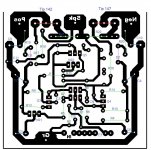
If you look at my layout you can see if I rotate the capacitors (next to the power transistors) I can use even 2200uFt to.
There is room enough there.
I will see if really necessary to go over 470uF what I think is a decent capacitor for that position.
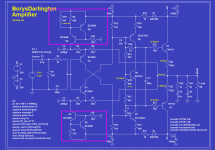
By the way these is the final layout what I will use at my tests.
The size of the PC board 86 X 82mm
86 wide frame to frame and 82 long.
Greetings
If the PS built on a PC board like many commercial amp we have to use what ever need for there.
If you look at my layout you can see if I rotate the capacitors (next to the power transistors) I can use even 2200uFt to.
There is room enough there.
I will see if really necessary to go over 470uF what I think is a decent capacitor for that position.
By the way these is the final layout what I will use at my tests.
The size of the PC board 86 X 82mm
86 wide frame to frame and 82 long.
Greetings
Attachments
Member
Joined 2009
Paid Member
Hmmm....I went off track around mid 2014 and never got back due to a lot of reasons plus side tracked by some new things that came along......usual rant ..
However I do want to complete my stereo version for which I had even bought the transformer and heat sinks ! I think I will do something this year ! In the meantime the L12-2 amp caught my attention . After many months I bought the boards recently on eBay. Making boards myself is becoming time consuming.
The L12 amp is very nice . Will have to compare that with your amp. Since there are some variations possible I'll pick the one I like best to test. Two important factors will be dc offset stability ( with fluctuating supply voltage ) and dc bias stability.
Cheers.
Any progress on this project, the dream should not end yet...
Hi
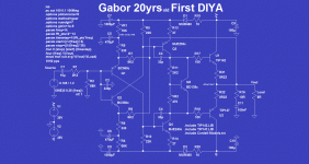
Mosquito simulated the VBE modified version the result he get is very bad.
With these tweak the sim result is (very) good but may be we back to the thermal drift problem.
Who knows

I think I will build these and if there will be problem try to solve it on the actual amplifier.
I waited until now so someone simulate the VBE molded circuit.
Now time to work on the layout and after turn on the soldering station.
Bigun or anyone else who interested please take a look at the latest circuit
Thanks
Attachments
Member
Joined 2009
Paid Member
I am happy to see this thread coming alive!
Still, I suggest somebody should run quick Spice sim with "TEMP 30 40" to see how stable is bias of output power devices with temperature. More sophisticated simulation needs control over individual devices of course but it's simple enough to do global test whilst you begin some real soldering!
I like this topology and I have reserved many pairs of Sanken Darlington devices for when time is available !
Perhaps good to add a capacitor across Vbe to ensure good a.c. Behaviour.
Hi
Bigun I agree with the capacitor across to the VBE
Very likely next to the VR2 we will need a resistor, one side it has 2K2 the other side only a 470VR.
At least for test I made the room for the mentioned components
The resistor marked as a J jumper the capacitor not marked but is there in the layout
Greetings
Attachments
One of my first builds was a Maplin amplifier in around 1980.
It was 225WRMS and I used it with four Fane 50WRMS speakers on a mobile disco.
It sounded very good and was very loud when required.
It was 225WRMS and I used it with four Fane 50WRMS speakers on a mobile disco.
It sounded very good and was very loud when required.
An externally hosted image should be here but it was not working when we last tested it.
Last edited:
Member
Joined 2009
Paid Member
You've lost me there Nigel, the Maplin circuit has no relevance in this thread??
How to provide thermal stability for Gabor's amp is the question. I think the issue as always is the VAS, the current through it increases with temperature and this simple Vbe causes increase in OPS current. The VAS emitter degenerate helps but may not be enough and increasing it will reduce OLG. Other option is to make the Vbe multiplier immune to VAS current using solution like my TGM5. Or add some temperature variable element to the input stage like VSSA. What other ideas - there are more options?
How to provide thermal stability for Gabor's amp is the question. I think the issue as always is the VAS, the current through it increases with temperature and this simple Vbe causes increase in OPS current. The VAS emitter degenerate helps but may not be enough and increasing it will reduce OLG. Other option is to make the Vbe multiplier immune to VAS current using solution like my TGM5. Or add some temperature variable element to the input stage like VSSA. What other ideas - there are more options?
You've lost me there Nigel, the Maplin circuit has no relevance in this thread??QUOTE]
The thread is about someones first am p2 0 years ago.
I just put forward mine from 35 years ago !
Simples !
Member
Joined 2009
Paid Member
Hi Bigun
These circuit very similar to the .....................!!!
You know first someone started here in the forum and after several DIY-ers got the idea - I mean borrowed the idea
Thank God because that helps a lot
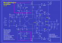
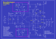
Basically these circuit used Toshiba 2SK1530 & 2SJ201, it is from Borys but I did modified to darlington with the assist of Boris
Boris tested these with IRFP mosfet and other power semis, based on his opinion the Toshiba version sounded the best..
The front of these very similar to the VSSA. The rest is identical (I mean at the layout ) only need to use the right value resisters or first give a try to these.
By the way these worth to be tested and to be compare to the beginner.
Do you think these would help with the thermal compensation
I do have layout for these to but I made it to use 2 pair darlington or Toshiba mosfet like 2SK1529 & 2SJ200.
Right now I do not interested on Toshiba devices, I got two AUSSIE module with 4 pair Toshiba fet.
Your opinion
These circuit very similar to the .....................!!!
You know first someone
started here in the forum and after several DIY-ers got the idea - I mean borrowed the ideaThank God because that helps a lot
Basically these circuit used Toshiba 2SK1530 & 2SJ201, it is from Borys but I did modified to darlington with the assist of Boris
Boris tested these with IRFP mosfet and other power semis, based on his opinion the Toshiba version sounded the best..
The front of these very similar to the VSSA. The rest is identical (I mean at the layout ) only need to use the right value resisters or first give a try to these
.By the way these worth to be tested and to be compare to the beginner.
Do you think these would help with the thermal compensation
I do have layout for these to but I made it to use 2 pair darlington or Toshiba mosfet like 2SK1529 & 2SJ200.
Right now I do not interested on Toshiba devices, I got two AUSSIE module with 4 pair Toshiba fet.
Your opinion
Attachments
post573
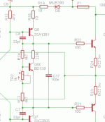
R20 is the Hawksford/Hagerman/Self added resistor to compensate the Vbe multiplier for variations in multiplier current.
As such the tappings to feed the next stage are connected to the emitter and collector of Q9.
The sch shows the upper tapping connected to the wrong side of R20.
C17 & R22 should connect to the bottom end of R20.
post573
R20 is the Hawksford/Hagerman/Self added resistor to compensate the Vbe multiplier for variations in multiplier current.
As such the tappings to feed the next stage are connected to the emitter and collector of Q9.
The sch shows the upper tapping connected to the wrong side of R20.
C17 & R22 should connect to the bottom end of R20.
Thank you Andrew
Three variation is possible but very likely only one is correct because You did not mentioned Q8 & Q9 Collector how to connect together...........
I had something similar earlier (a few page back) with a extra diode together, at the simulation it did not work at all
These circuit was made by Borys and in real life it performed very well, that not mean everything was connected correct!
Here is the modified circuit
Please let me know which one you think out of the three version is more acceptable
Thank you very much
Attachments

post573
R20 is the Hawksford/Hagerman/Self added resistor to compensate the Vbe multiplier for variations in multiplier current.
As such the tappings to feed the next stage are connected to the emitter and collector of Q9.
The sch shows the upper tapping connected to the wrong side of R20.
C17 & R22 should connect to the bottom end of R20.
It looks like it can be some controversy about that..
Attachments
It looks like it can be some controversy about that..
It would be nice to clear that out. I can not ask you please simulate all 3 so see which would be the right connection.
I know Bigun also advised something like the first out of the three I posted with an extra diode but that simulated bad.
Maybe because the diode
I don't know
Lets wait if someone has more idea
Greetings
Member
Joined 2009
Paid Member
I'm in Paris (the real one, not Ontario) at the moment with no access to simulations. If I remember correctly the Haggerman simulated just fine for me with the right choice of resistor values. He has a websit that shows a few Vbe variations.
edit: http://www.hagtech.com/pdf/vbe.pdf
The key with the CCS front end is to thermally couple ONE of the transistors of each CCS to the power output devices; you will see how I did this very neatly with my TGM7 amplifier PCB. It would be helpful to simulate first, alas I can't at the present time.
You may not need both design elements and I suspect the thermally coupled CCS is the better option.
Last edited:
- Home
- Amplifiers
- Solid State
- My first DIY amplifier 20 years a go