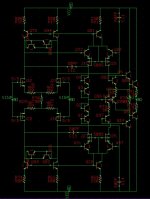
In checking the data sheet after a comment here I realized how simple this circuit might look in a fully complementary process. Not much optimization yet, I don't think these values are unity gain stable and it appears to phase invert when slammed into the plus rail (could be my models). I simmed it with some fairly ordinary npn's and pnp's and SK170/SJ74 models and got -150dB in the 3V rms into 600 Ohm condition at G=11 off of the datasheet. I ran this at 25mA though so as not as JC would say "choke it like a chicken".
Something here for the "real' op-amp guys too AOL >1e6 and the usual single pole behavior so the gobs of feedback are available") .
.
I added the VAS that "chases its own tail" so this whole circuit lights up with only the input stage current. Truly no use of ground inside the circuit for bypass of bias rails or cascodes. The FET cascodes in the output might be better as bipolars but that adds a need for a place to tie the bases.
This looks like a nice candidate for a little amp on a card that could pop into many of the OPA627 phono circuits for some BA style listening fun.
No IP (that I know of) here so anyone is welcome to have fun if they feel inspired. No stones please. If this is already out there, sorry, I didn't make a search.
Something here for the "real' op-amp guys too AOL >1e6 and the usual single pole behavior so the gobs of feedback are available
.I added the VAS that "chases its own tail" so this whole circuit lights up with only the input stage current. Truly no use of ground inside the circuit for bypass of bias rails or cascodes. The FET cascodes in the output might be better as bipolars but that adds a need for a place to tie the bases.
This looks like a nice candidate for a little amp on a card that could pop into many of the OPA627 phono circuits for some BA style listening fun.
No IP (that I know of) here so anyone is welcome to have fun if they feel inspired. No stones please. If this is already out there, sorry, I didn't make a search.
Attachments
john curl said:Looks good, Scott! Now, let's make these things, and the consumer audio world will be at your door.
The seventh was about -200dB!
scott wurcer said:In checking the data sheet after a comment here I realized how simple this circuit might look in a fully complementary process.
Very interesting Scott, this is something I was looking for in a previous post, thanks
Now I may need to redraw the schematic but:
- how does this circuit start (bias wise) at power up?
- it seems like it's latching to the rails, following an overload condition?
- Q1...Q4 is this practical for a discrete implementation?
- same for Q71/Q90 and Q88/Q91
Any noise estimates?
Am I wrong or chances to integrate such, due to the lack of a compatible complementary process, are slim...?
BTW, OPA687 is gone for good, OPA847 is the replacement, but that's not FET input.
Those diode connected devices could be just diodes or maybe just left out. Q1-4 just balance the voltage drops fastidiously and could be dropped. The latch up needs to be addressed, there might be a simple clamp that works. The quad of FET's is self starting, in fact in the old days an EPI FET was often used for startup. The diodes across the second stage stop one obvious misbehavior. You are also right in that complimentary IC FETs are a fantasy, the P would probably be a curiosity at best (or visa versa of course). The N's are native to our SOI proceses while P's are native in the old days.
Ramping the supplies and saving all the node voltages and currents gets it to converge the next time with supplies turned on all the way.
Ramping the supplies and saving all the node voltages and currents gets it to converge the next time with supplies turned on all the way.
scott wurcer said:The quad of FET's is self starting, in fact in the old days an EPI FET was often used for startup.
Yep, sorry, I forgot for a sec it's JFET input. Of what I can recall, I think uA723 was using an EPI FET to bias the circuit at power up (and then bias the reference).
Yikes!
Perhaps I'm missing something, but I can't see this thing working with real life discrete parts without a CMCL.
Those current source/mirror loaded LTP have so much DC gain with the slightest imbalance/component mis-match the thing will never bias up right.
Cheers,
Glen
Perhaps I'm missing something, but I can't see this thing working with real life discrete parts without a CMCL.
Those current source/mirror loaded LTP have so much DC gain with the slightest imbalance/component mis-match the thing will never bias up right.
Cheers,
Glen
I'll tell you this, Scott. If I were to make a high feedback, moderate open loop gain amp, I would choose your circuit. Another related approach is to make a 12dB/octave internal rolloff and get the open loop response way up. I did a design for Sound Technology that had a 100KHz open loop bandwidth and max feedback. This topology might not go that far, but 10KHz would be interesting, and then max feedback. I am just pointing this out for discussion. Still, I am proud of you, as you have seen the light. Dick Sequerra says hi.
G.Kleinschmidt said:Yikes!
Perhaps I'm missing something, but I can't see this thing working with real life discrete parts without a CMCL.
Those current source/mirror loaded LTP have so much DC gain with the slightest imbalance/component mis-match the thing will never bias up right.
Cheers,
Glen
Glen, If you notice the outside halves of the differential VAS have an excape path for current out the emitters of the darlington to the rails. Yes the amp has to become differential to single ended somewhere or it's like paralleling two op-amps and having the input offsets fight. Offsets then make these two currents slightly unequal while the loop forces the currents into the high gain node to be equal (within Ib matching etc.)
I definately will try building one since I have all the parts around. If successful I'll bring a couple to the next BA.
john curl said:I'll tell you this, Scott. If I were to make a high feedback, moderate open loop gain amp, I would choose your circuit. Another related approach is to make a 12dB/octave internal rolloff and get the open loop response way up.
I'd add a CMCL (common mode control loop) so that it could actually work first.
Suppose that the N channel “LTP” is made with perfectly matched parts; the quiescent currents in each leg are perfectly balanced with both differential inputs (+/-) at 0V.
Now suppose that the P channel “LTP” parts are not perfectly matched; the currents in each leg are only equal when there is a +2mV DC offset voltage applied to the differential inputs.
Now what happens when the NFB loop attempts to steer this P channel “LTP” into balance? – the N channel “LTP” is thrown way out (due to the huge DC gain 2mV input is much more than enough to overdrive the second stage).
Cheers,
Glen
scott wurcer said:
Glen, If you notice the outside halves of the differential VAS have an excape path for current out the emitters of the darlington to the rails. Yes the amp has to become differential to single ended somewhere or it's like paralleling two op-amps and having the input offsets fight. Offsets then make these two currents slightly unequal while the loop forces the currents into the high gain node to be equal (within Ib matching etc.)
I definately will try building one since I have all the parts around. If successful I'll bring a couple to the next BA.
Hi
The VAS is not where I see the problem - it's with the required balance of the complementary first stage. I'm pretty sure I've got it right.
I explained the issue in another post prior to your reply above, which hasn't appeared yet as my posts are under moderation.
I suspect it will appear at the same time as this one.
Cheers,
Glen
Scott,
Very nice circuit, but would be difficult to fit into a DIP8 footprint ??
This was my attempt and I had a hard time fitting in 7 active devices (SOT23) :
http://www.diyaudio.com/forums/showthread.php?s=&threadid=120445&highlight=
Perhaps you would also come up with one using (less no.of) SMD components, such as BF862, etc. ??
Best regards,
Patrick
A little egg left on my face this morning. Glen you are somewhat right. I'm not set up for Monte Carlo at discrete tolerances. The circuit is surprisingly robust to IC tolerances after laser trim, but a discrete would require a few trim pots or offset servo.
You would think there was no tolerance at all but .1-.2% shifts seem Ok, this is orders of magnitude worse than I am used to.
Before I went over the cliff to this totally symetrical design I was working on something Friday that would be more discrete friendly. I'll resurect it.
Forgive a little Sunday whiteboarding.
G.Kleinschmidt said:
I'd add a CMCL (common mode control loop) so that it could actually work first.
Suppose that the N channel “LTP” is made with perfectly matched parts; the quiescent currents in each leg are perfectly balanced with both differential inputs (+/-) at 0V.
Now suppose that the P channel “LTP” parts are not perfectly matched; the currents in each leg are only equal when there is a +2mV DC offset voltage applied to the differential inputs.
Now what happens when the NFB loop attempts to steer this P channel “LTP” into balance? – the N channel “LTP” is thrown way out (due to the huge DC gain 2mV input is much more than enough to overdrive the second stage).
Cheers,
Glen
G.Kleinschmidt said:
Hi
The VAS is not where I see the problem - it's with the required balance of the complementary first stage. I'm pretty sure I've got it right.
I explained the issue in another post prior to your reply above, which hasn't appeared yet as my posts are under moderation.
I suspect it will appear at the same time as this one.
Cheers,
Glen
EDIT:
After doing some calculator button pushing I think you might be saved from the need of a CMCL. The VAS which does not have emitter degeneration and is not preceeded with a EF buffers to lighten the load on the input stage keeps the input stage gain down. The low gm of the Jfet input pairs also helps things here.
I think it might still be touchy though WRT to "offset fight".
In my experience with circuits like these a maximum gain of about 40dB can be had from the first stage - but matched dual-die / array input devices and resistor trimming to null out the offsets is critical to keep the whole amplifier well balanced.
If you really want more than 40dB of first stage gain then a CMCL is pretty much mandatory - like in Edmonds PGP amp.
How much DC gain does the simulator give you for the first stage?
I'd add a mV voltage source in series with one of the input jfet source pins to simulate a realistic Vgs mismatch and check the quiescent currents in all legs (LTP/VAS) of the amplifier to see just how much the balance is thrown out.
Cheers,
Glen
scott wurcer said:Glen, thank's again for your comments. It looks like a simple gain killer for the first stage (2K 's across the drains of the FETs) seems make the offset pretty robust without much compromise to the circuit. A simple offset trim should do now.
I almost suggested resistive drain loads, but I wasn’t sure how prepared you’d be to super-match jfet pairs
However this leads to a quandary;
If it transpires that a 2k load resistance is necessary to mitigate offset imbalance how do you justify the extra complication of those current source input stage loads?

Glen
G.Kleinschmidt said:
I almost suggested resistive drain loads, but I wasn’t sure how prepared you’d be to super-match jfet pairs
However this leads to a quandary;
If it transpires that a 2k load resistance is necessary to mitigate offset imbalance how do you justify the extra complication of those current source input stage loads?
Glen
This would be instinctive because the gain is reduced without a headroom drop. More work tonight and I think it will come around, no more latchups, picture perfect 20V p-p 100k sq waves @ g=2. These everything floating circuits have some strange properties,for instance the AOL is still 140dB with the 2k resistors. I won't bother anyone again till I test it out.
Patrick,
Abot absolute DC offset and speaker protection on aleph-x...
I found this for balanced speaker protection circuit on aleph-x thread. IF this operate when absolute DC offset several volts,
I mean that realy is on position at high absolute DC offset...
I have to use this circuit. But I can't read exact zener value and constant current IC. Please let me know.
Regards,
Chois
Attachments
- Status
- This old topic is closed. If you want to reopen this topic, contact a moderator using the "Report Post" button.
- Home
- Amplifiers
- Solid State
- Discrete OPA627/687?