Hi,
I've just finished building a pair of p3a using 2n5551, mje350/340 and tip3055 and tip2955. I've designed my own pcb's using the schematics posted on Elliot's web site.
It works nice. I correctly set the Iq, and checked all connections and voltages several times.
I tried it for several hours. No problems at all. No heat problems, no sound problems.
Then, I removed the tip3055 and the tip2955 and replaced them with toshiba transistors 2sc5200 and 2sa1943. They shorted within minutes of testing. It happened twice: they worked for a few minutes, then after powering off and then back on, they shorted badly.
Should I make any mod to the amps to make them work or could them just be fakes?
Thanks in advance for your comments.
Best Regards,
Guido.
Guys Come On !!!!!!!
VERY SIMPLE
when you replaced the transistors you need to do again idle adjustment .....from scratch
may be 1943+5200 are better transistors but they are not "drop in " replcements ....
i will be very happy to see your pcb .....
in my testings BD139-140 sounded better than 340-350
if your transitors are fake they will probably work fine ...but only up to a low level of power and load .....push them a bit harder and then boooooom !!!!!! be carefull about that also
yet again same story .....
people miss the obvious and look on satelites that might go to mars ......i am breathless ....
Lumba Ogir said:markoramius,
Oscillation!
people miss the obvious and look on satelites that might go to mars ......i am breathless ....
Two other possibilities:
1) Your PCB layout is not good enough. The P3A uses a CFP output, and this is notorious for oscillation - the PCB design is crucial here. Long traces between the drivers and the outputs is a no-no.
2) Your transistors are fakes, without meaning to sound bad, this is quite likely considering where you are from
If you have not put it on your design, put some small electrolytic decoupling caps near the output transistors, say 330uF. They should be near to the output transistors, as should the 100nF decoupling capacitors Elliot shows.
You cannot set the bias with one pair of output transistors, and then swap in another. You must start with zero bias and bias them with the new pairs.
I would recommend MJE350 for VAS, and BD139/140 for drivers.
I've used 2SA1943 / 2SC5200 on Rod's earlier P3A boards and experienced no problems. The miller caps were standard value and used silver mica.
It's been mentioned but VR1 needs to be set for max resistance and safety resistors installed and then go through the complete checks and biasing procedures.
It's been mentioned but VR1 needs to be set for max resistance and safety resistors installed and then go through the complete checks and biasing procedures.
Hi,
Thank you all for your replies.
I read a lot thru the forum about oscillation. I tried to do things in order to avoid it.
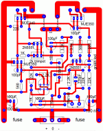
Sakis: thanks, I'm posting pcb layout here. I would really appreciate to hear your comments about it (please be gentle, this is my first diy audio project!!!). Small transistors are 2n5551. Input cap is 4u7 polyester. C2 / C4 / C6 are ceramic disc capacitors: I KNOW THEY ARE NOT RECOMENDED, but I couldn't find a supplier for better materials.
When I've installed the toshiba pair I performed the Iq adjustment with patience, according to Mr. Elliot's project web page.
Jaycee: I know the layout is crucial. It is my first. Maybe is no good at all. I read a lot thru the forum and looked at several examples and things to take into consideration. Regarding the transistors, I suspect they were not original, because of price and appearance. The 2sc5200 didn't say toshiba at all.
Thank you again for your posts. I really enjoy doing this project and learning a lot while I'm doing it. I hope to make it work.
Best Regards,
Guido.
Thank you all for your replies.
I read a lot thru the forum about oscillation. I tried to do things in order to avoid it.
Sakis: thanks, I'm posting pcb layout here. I would really appreciate to hear your comments about it (please be gentle, this is my first diy audio project!!!). Small transistors are 2n5551. Input cap is 4u7 polyester. C2 / C4 / C6 are ceramic disc capacitors: I KNOW THEY ARE NOT RECOMENDED, but I couldn't find a supplier for better materials.
When I've installed the toshiba pair I performed the Iq adjustment with patience, according to Mr. Elliot's project web page.
Jaycee: I know the layout is crucial. It is my first. Maybe is no good at all. I read a lot thru the forum and looked at several examples and things to take into consideration. Regarding the transistors, I suspect they were not original, because of price and appearance. The 2sc5200 didn't say toshiba at all.
Thank you again for your posts. I really enjoy doing this project and learning a lot while I'm doing it. I hope to make it work.
Best Regards,
Guido.
Attachments
i am pretty sure
that when you poewered up your amp idle was on maximum thatswhy you fried the transistors ....
and/or your calculations about idle were wrong .....
thats ok though we all been in this mistakes more than once ....
i also made my own pcb since i had my own criteria about it and the best i ve heard about this amp after many many tests was the version that included 68pf multileyer vas cap .... notorola bd 139 and 140 military specs and original 2SA 1302 -3281 toshiba transistors .....
the think is that i have accses to many weird semiconductors and still have left about 150 pairs of these output transistors originall made .... so a get the chance to play arround with difrent kinds of semis ....
once i try to see if there is audible diference between bd139-140 of philips and st ....philips sounded better but may be i am worng .... then again compaired to all these i have from a police stock ...original motorola's bd 139-140 gold plated tips sounded the best !!!!!
i plan to use them in the future in my own amps ....NOT for sail OR for costumer repairs ....
finally i agree with jay cee that pcb is critical for this amp ( others also ) and ground rooting signal returns and so on can make a big diference .... for shure rods pcb will be one of the best options ( also costs nothing )
at least by this way you are on the safe side about a lot of things
by the way
nice nick name ....""""" marko ramious """"" skipper of the red october ....
a movie i ve seen 50 times i will be very glad to see it another 50 ha ha ha .....may be in the future .....
me and sziklai sitting together having beers and watching red october ...... ha ha ha !!!!!
nice nick name ....""""" marko ramious """"" skipper of the red october ....
a movie i ve seen 50 times i will be very glad to see it another 50 ha ha ha .....may be in the future .....
me and sziklai sitting together having beers and watching red october ...... ha ha ha !!!!!
markoramius said:C2 / C4 / C6 are ceramic disc capacitors: I KNOW THEY ARE NOT RECOMENDED, but I couldn't find a supplier for better materials.
Rod's board buyer's assembly instructions do have ceramics listed for C2, C4, C6 but recommends 500V for C4, C6 as they are better on handling higher frequencies I think. I've used 50V ceramics in all these locations and were fine IMO.
Not having Toshiba written on the devices is not a good omen. There's some posts around here on what they are supposed to look like and comments on the fakes.
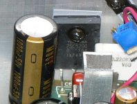
I've attached a pic of the real Toshiba that I used in my DX amp.
Attachments
Not necessarily, most times I have found to have oscillation problems when using fakes or second source chinese manufactured devices while original devices dont suffer from this. Unfortuneatly I dont have the equipment to test these devices to find exactly what it is that makes them prone to oscillations.
the pcb
i dont thing that the pcb is that bad ....
there is an amount of things that i would do diferent way .....
cant say for sure but after a very quick look i think that has no mistakes circuitwise ....
a few comments
i like very much that ltp can have thermal contact thats a principal i like very much
but otherwise i think eventhough i like the pcb since its square and symmetric after a second look there is a lot of thing i did diferent
----output cap and resistor (part of zobel) needs to stay away from the input ( in my amps this part is in the output contacts and the return to ground is with a seperate cable to star ground )
---- It could be an option that 2N5551 could have thermal contact with one of the drivers to aytomaticly adjust idle ( might be handy in case your amp is pushed to the limits or more )
----it is prooven that in audio too many parallel lines and too many corners effect sound
----- it could be done smaller yet the same nice nad symmetric
----- for the particular circuit the decoupling network of 100nf +100mf for + and - rails is better to beplaced as close is possible to output and drivers
------ finally star ground philosophy can also apply when we design pcb for audio ..... returns to star ground avoid oscilation and formation of capacitance between traces
now days i prepair one version with all the above goodies plus psu capacitors located just next to outputs and drivers ....will construct and let you know
***** not to make you disapointed your pcb might play very fine .... but if you have time for more diy you might construct under these roules and then you see on your own
Hi,
Thank you all for your comments.
I realize now how critical is the pcb layout, grounding and all the considerations to take into account in order to successfully build this project. I will keep trying to improve all this, following all your helpful tips.
Sakis, thank you very much for commenting on my pcb. I'll give a try to your important recommendations. By the way, The hunt for the Red October is the best movie of all times!!! Good luck on the p3a you told you will start to build soon. I hope to hear your progress on that one.
Rabbitz, thank you for the image. The transistors I had (I threw them away immediately, I got very angry then) were not alike the one in the photo. I'm having a hard time finding a source for good stuff.
Jaycee, ok with decoupling caps. Will use 330 uF on the next one near the output transistors just as Sakis also said.
One last question: I saw some images here and there of some p3a amps built with R13 and R14 at 0.47 ohm while on the schematics is stated 0.33 ohm. Was there some upgrade?
Thanks again for you kind assistance.
Best Regards,
Guido.
Hi Guido,
As pointed out by a couple of posters, the layout with the CFP is abosolutely critical between the driver and output device as these two work together in providing local feedback, the longer the trace the more potential for unwanted inductance, capacitance. Also the proximately between traces surrounding this pair can affect the performance and lead to oscillation. Shorting output is pretty drastic and means that the op transistor is burning up after getting very HOT!, also with the drivers, ideally you want these to be faster(higher gbw) than the output devices in the CFP, unfortunately I find no reference to this in the datasheets...
Colin
markoramius said:
One last question: I saw some images here and there of some p3a amps built with R13 and R14 at 0.47 ohm while on the schematics is stated 0.33 ohm. Was there some upgrade?
/B]
0.33 is what Rod recommends, but 0.47 is more commonly available - both will work, the 0.47 just loses a little more power.
- Status
- This old topic is closed. If you want to reopen this topic, contact a moderator using the "Report Post" button.
- Home
- Amplifiers
- Solid State
- p3a blowing 2sc5200 / 2sa1943 problem