thanks, Stee
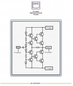
nice schematic
what tests have you done:
- as buffer, Gv=1
- at Gv=10 (+20dB)
- with different loads
- with different input AC levels
- with different output AC levels
- with different Voltage Supply
what is the recommended nominal Power Supply to use?
2 x 20 VDC max ... or
what transistors you use - you recommend
NPN? PNP?
thanks lineup is interested
nice schematic
what tests have you done:
- as buffer, Gv=1
- at Gv=10 (+20dB)
- with different loads
- with different input AC levels
- with different output AC levels
- with different Voltage Supply
what is the recommended nominal Power Supply to use?
2 x 20 VDC max ... or
what transistors you use - you recommend
NPN? PNP?
thanks
lineup is interestedStee
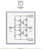
I see you have already this GAS amplifier schematic
at your website
http://www.esafono.it/hindex_file/image003.jpg
http://www.esafono.it/hindex.htm
Have you joined my Audio Forum?
here it is http://lineupaudio.freehostia.com/forum/index.php
very small forum - me as moderator
We can post New Project & Discuss your GAS.
then later we come back here to www.diyaudio.com
and present our result from Project design!
===================================
Click my www below my post
= audio forum ... easy to join
Hi lineup
never tested, it's a fresh idea
think is better use power bipolar as 2SA5200 & C TOSHIBA
and his drive can be MJE340 & C
just to start at Gv=10 (+20dB) with dual 30V
do you have a simulator?
Regards
lineup said:thanks, Stee
nice schematic
what tests have you done:
- as buffer, Gv=1
- at Gv=10 (+20dB)
- with different loads
- with different input AC levels
- with different output AC levels
- with different Voltage Supply
what is the recommended nominal Power Supply to use?
2 x 20 VDC max ... or
what transistors you use - you recommend
NPN? PNP?
thanks
never tested, it's a fresh idea
think is better use power bipolar as 2SA5200 & C TOSHIBA
and his drive can be MJE340 & C
just to start at Gv=10 (+20dB) with dual 30V
do you have a simulator?
Regards
about better sound
GAS is an ambitious project
to have Class A sound with AB class biasing
without bridge and OPA
with complementary and balanced criterion
in very simply design
I have found now a good simulator
http://www.catena.uk.com/cgi-bin/download1.pl?id=125930
GAS is an ambitious project
to have Class A sound with AB class biasing
without bridge and OPA
with complementary and balanced criterion
in very simply design
I have found now a good simulator
http://www.catena.uk.com/cgi-bin/download1.pl?id=125930
Eagle & B2 Spice & LTspice
I have installed SIMetrix maybe 2 months ago.
I have not learned how to use.
Have we some good transistors in SIMetrix?
What we want is simulation software (freeware)
with many AUDIO transistors, mosfet and bipolar.
People often use these free simulators & schematics designers:
- LTspice/SwitcherCAD III
http://www.linear.com/designtools/software/
- Eagle CADsoft
http://www.cadsoftusa.com/freeware.htm
- B2 Spice A/D v4 Lite, which can work with Eagle
http://www.beigebag.com/adv4_lite.htm
How to build a schematic in Eagle and export it to B2 Spice A/D v4 for simulation:
http://www.beigebag.com/eagle.htm
Lineup
Lineup Audio Blog & Audio projects Forum for members
I am sure GAS and also UAS will work well.
You do work now. Will later be final versions.
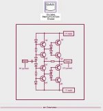
Did see you have a nice circuit here (UAS)
http://www.diyaudio.com/forums/attachment.php?s=&postid=1587901&stamp=1219024318
2SJ160 / 2SK1056 as driving 2SC5200 / 2SA1943
... this is a new idea for me .. but think is not bad
maybe will work perfect!
Lineup
http://lineupaudio.freehostia.com/forum/
You do work now. Will later be final versions.
Did see you have a nice circuit here (UAS)
http://www.diyaudio.com/forums/attachment.php?s=&postid=1587901&stamp=1219024318
2SJ160 / 2SK1056 as driving 2SC5200 / 2SA1943
... this is a new idea for me .. but think is not bad
maybe will work perfect!Lineup
http://lineupaudio.freehostia.com/forum/

Are you trying to design something that looks good as a schematic (very symmetrical) or something that actually works?
Your cut and past from other people's schematic, without quoting the authors, won't make you a more experienced designer. Don't think I didn't recognize the cut and paste from Elliott, in the schematic from the other topic.
Your cut and past from other people's schematic, without quoting the authors, won't make you a more experienced designer. Don't think I didn't recognize the cut and paste from Elliott, in the schematic from the other topic.


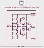
actually after i got time to look at i did find one such "fallacy" with the circuit. look at the center vertical string of diodes and transistors. there are 4 diode drops between each rail and the center point. so the center point wants to be at 2.8 volts from each rail. while this circuit might work with +/- 3V rails(and i say might, because i was just scanning it by eye first for obvious "oopses", and not yet looking at actual operational mechanisms), much higher than that will definitely let the magic blue smoke out of these components. operationally, it looks as if the middle section is a problem again here. there is no net change of conduction here between the rails and the center point, so the center point will tend to hover around zero. even if there were a change in conduction, you have the diode drops swamping what little net changes in conduction you do get. what should be a high impedance node (the VAS) is shunted by a very low impedance (the diode drops. the actual high impedance nodes in this middle stage are the collector connections, just like in the first stage, and being a second inversion (the first inversion takes place in the first stage) follows the input signal. well, that's what i can see taking a closer look at it, if somebody has modeled this, please pu your $0.02 in. if nobodey does, then i'll model it tomorrow and see what happens. as i suspected though, it is a lot like the "dual bridge" rectifier circuit with a high potential for pyrotechnics. the "dual bridge" is a classic. take 2 bridge rectifiers and put them in series (connect an ac pin of one to an ac pin of the other, then connect the remaining ac pins across a transformer secondary). then connect the middle (the two interconnected ac pins) to ground, creating an artificial ground. then connect the negatives together and the positives together for the rails. you now have a fire hazard. if you draw it out with diodes, you will see a very direct path (well, sort of, it actually zigzags through the bridges)through the diodes across the transformer secondary
actually after i got time to look at i did find one such "fallacy" with the circuit. look at the center vertical string of diodes and transistors. there are 4 diode drops between each rail and the center point. so the center point wants to be at 2.8 volts from each rail. while this circuit might work with +/- 3V rails(and i say might, because i was just scanning it by eye first for obvious "oopses", and not yet looking at actual operational mechanisms), much higher than that will definitely let the magic blue smoke out of these components. operationally, it looks as if the middle section is a problem again here. there is no net change of conduction here between the rails and the center point, so the center point will tend to hover around zero. even if there were a change in conduction, you have the diode drops swamping what little net changes in conduction you do get. what should be a high impedance node (the VAS) is shunted by a very low impedance (the diode drops. the actual high impedance nodes in this middle stage are the collector connections, just like in the first stage, and being a second inversion (the first inversion takes place in the first stage) follows the input signal. well, that's what i can see taking a closer look at it, if somebody has modeled this, please pu your $0.02 in. if no
- Status
- This old topic is closed. If you want to reopen this topic, contact a moderator using the "Report Post" button.
- Home
- Amplifiers
- Solid State
- GAS - Global Amplification Stage