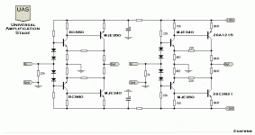
Hello to All
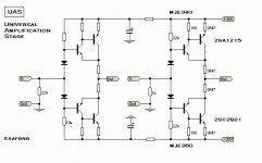
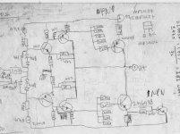
I will present my recent idea - the UAS
This amplifier has the ability to govern themselves alone
thanks to local feedback on output resistors
it's esoteric because ultra simple
it's complementary
can build in chain with different power
need matching devices
do not need adjustment
have gain in voltage and in current
can use LED for biasing
between pre and final stages better put a potentiometer
its natural evolution provides the drive with mosfets
do you think it's intresting?
never tested
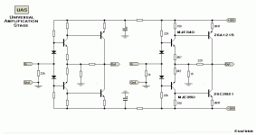
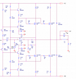
Attachments

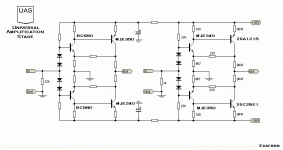
you can add one film capacitor
across those 2 input diodes
... from base to base of input transistors
will act as a sort of BOOTSTRAP
something like 1 uF would maybe be suitable
otherwise I think your amplifier is a very nice idea
more creative and interesting
than most I can discover at this board from other posters
")
across those 2 input diodes
... from base to base of input transistors
will act as a sort of BOOTSTRAP
something like 1 uF would maybe be suitable
otherwise I think your amplifier is a very nice idea
more creative and interesting
than most I can discover at this board from other posters
Guthorst said:It will have very high THD because of the full class B bias setting.
And there is NO negative feedback.
regards,
Guthorst
... but there is a LOT of nfb. And the biasing is probably class AB. But that's easy to set with some resistor values.
My question is more, what's 'universal' about this?
Jan Didden
Hi Janneman
I called Universal
because as for OPA
is a model that you can repeat the same at every level of power
does not require settings - so it is configured with a standard, perhaps an integrated
also evades the tradition that wants to always be the mirror of current in input
bias control in VAS
and the output stage only in current gain
also has the ambition to become globally esoteric
because extremely simple (perhaps sounds good)
you may have to hold a conference to AES in New York...
the only new idea (I think)
is to use a shunt to monitor the current on each branch
in very short rings
I hope also become Universal with your contribution
maybe a good idea use FET/Mosfet in input...
Regards and Thanks
Hi lineup
thanks a lot for your support
this 1uF film capacitor from base to base it's for RF filter?
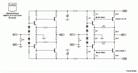
Attachments
Cross-conduction means current flowing from the positive supply rail to the negative supply rail because both banks of output devices are conducting at the same time.
It happens because in bipolar transistors collector current does not stop immediately when base current is removed, it takes a few dozen microsedonds to fall to 0. A negative base current is required in order to stop conduction quickly, which this circuit can't provide.
It happens because in bipolar transistors collector current does not stop immediately when base current is removed, it takes a few dozen microsedonds to fall to 0. A negative base current is required in order to stop conduction quickly, which this circuit can't provide.
lineup said:thanks Eva
how do we deal with this?
I mean we sometimes see one capacitor used 'to suck' out base current
from output bipolar devices
connected base-to-base in complementary follower output stages
is that one of tricks?
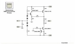
Yes and it works pretty well for EF output stages.
For CFP, it's more complicated. Here's a possible solution that I am looking into, for a MOSFET CFP stage (take this as a concept only). Note the bipolar drivers that can both source and sink current from the MOSFET gates.
Attachments
lineup,
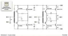
Class A biasing is the only way to avoid the highly disagreeable esoteric UAS cross-over distortion.how do we deal with this?

- Status
- This old topic is closed. If you want to reopen this topic, contact a moderator using the "Report Post" button.
- Home
- Amplifiers
- Solid State
- UAS - Universal Amplification Stage