Hi all.
I've been writing the CCS page on the wiki and I suddenly realized how a CAS works.
Now, if you're wondering why I was writing on the wiki about CCSs when I didn't understand the basic class-B/AB CAS, maybe you should check my work (a subtle hint to help me flesh out the wiki).
Most commonly in a CAS, the signal path is not separate from the output path, so voltage gain is zero. The togetherness of the signal and output paths makes NFB relatively simple: high-gain configurations (like the CFP) work quite well.
Now I present to you a low-power CFP Class AB output stage. C1 helps push/pull action, though a resistor in series might be beneficial. Quiescent current is theoretically about 27mA. Perhaps class-A is more practical for lower power like this but at least it shows I know something. THD at 1KHz is decent, especially with a 10k load.
I'm sure there's some tweaks I could make. You experienced readers feel free to educate me.
- keantoken
Attachments
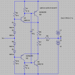
Q1 and Q2 should only need 1 diode drop each to turn on. What happens if you remove D3 and D4, and switch R5 and R7 to something lower (2.2 ohms?)
I think the natural extension of this would be a CFP diamond buffer: replace R3/R10 with CCSs, and the diode string with another pair of emitter followers.
I think the natural extension of this would be a CFP diamond buffer: replace R3/R10 with CCSs, and the diode string with another pair of emitter followers.
CBS240 said:Hmmm
Looks to me like the current that the 47uf cap takes to charge to rail to rail voltage will have to come from the bases of the output transistors. This = output saturation for the time the cap is charging which most likely with BJT's = crispy, fried silicon chips.
Definitely true. Maybe a much smaller (pF range) cap or no cap is better. As shown, the 22 ohm resistors will limit the current; it probably won't blow up on a real board, but it still isn't good.
I would put a resistor in series with the 47u, say 3.9k or something like that.
Yes, the transistors only need one diode drop each however I don't want to get it too close to class B amplification.
Yes, R3/R10 can by CCS's and they can also supply the input. An emitter follower/rubber diode replacing the diodes and we will have adjustable quiescent or bias current.
Funny how one thing makes sense and then suddenly it's all elementary.
Here is a zener for quiescent bias at ~50mA, current mirrors/source for input. Haven't sim'd yet, but I don't see why it wouldn't work.
- keantoken
Attachments
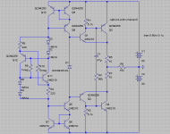
With R3=56K I don't think C1 will do anything. Consider that its time constant (where the capacitor is halfway "kicking in") is 2.63 seconds, and that the original purpose of C1 was push-pull drive of the output Qs' bases at high frequencies. What you want there is a small capacitor with no series resistance (or inductance) - a few pF would do, try 100pF for starters. I don't think it is necessary at all though. Also, where is the signal input?
BTW, I have had very good results in many circuits using a simple JFET ccs - just tie the source and gate together and it will pass Idss, which is usually in the right range - 2-20mA depending on the FET. They don't match well but it is usually AC performance that matters, not DC. You can also get away with all N-channel JFETs, even in an otherwise complementary circuit; the component matching in such a circuit has to be better than mixing N and P-JFETs.
The problem with running higher DC across the bases of Q1/Q2 is that you will need higher valued resistors for R5/R7 to reduce the idle current to something managable. With a single diode drop per output device, you can just use an ohm or two (or less on bigger devices); the output impedance is lower.
By the way, I just saw that your output devices are TO-92s. Watch out for the maximum dissipation on those! With +/- 30v rails, as you show, at 50mA bias, Q3 and Q4 will be dissipating 1475mW each. Q3/Q4 are going to go boom. Even at +/-12v as you showed originally, you'd be running 575mW - still a recipe for melted TO-92s. For TO-92s it's probably best to stay at or under 100mW - this will be a 20C rise over ambient temperature. Therefore, your idle current needs to be much lower.
BTW, I have had very good results in many circuits using a simple JFET ccs - just tie the source and gate together and it will pass Idss, which is usually in the right range - 2-20mA depending on the FET. They don't match well but it is usually AC performance that matters, not DC. You can also get away with all N-channel JFETs, even in an otherwise complementary circuit; the component matching in such a circuit has to be better than mixing N and P-JFETs.
Yes, the transistors only need one diode drop each however I don't want to get it too close to class B amplification.
The problem with running higher DC across the bases of Q1/Q2 is that you will need higher valued resistors for R5/R7 to reduce the idle current to something managable. With a single diode drop per output device, you can just use an ohm or two (or less on bigger devices); the output impedance is lower.
By the way, I just saw that your output devices are TO-92s. Watch out for the maximum dissipation on those! With +/- 30v rails, as you show, at 50mA bias, Q3 and Q4 will be dissipating 1475mW each. Q3/Q4 are going to go boom. Even at +/-12v as you showed originally, you'd be running 575mW - still a recipe for melted TO-92s. For TO-92s it's probably best to stay at or under 100mW - this will be a 20C rise over ambient temperature. Therefore, your idle current needs to be much lower.
AndrewT said:what the F... is a CAS?
That was my first reaction too. I guess it stands for Current Amplification Stage. Another addition to the TLA glossary.I guess it stands for Current Amplification Stage.
Yup.
By the way, I just saw that your output devices are TO-92s. Watch out for the maximum dissipation on those! With +/- 30v rails, as you show, at 50mA bias, Q3 and Q4 will be dissipating 1475mW each. Q3/Q4 are going to go boom. Even at +/-12v as you showed originally, you'd be running 575mW - still a recipe for melted TO-92s. For TO-92s it's probably best to stay at or under 100mW - this will be a 20C rise over ambient temperature. Therefore, your idle current needs to be much lower.
Yes, for lack of knowing any good high power pairs. I guess I'll try the bd139/140.
why does the schematic in post 1 show 27mA passing q3 but only 0.1mA passing q2?
No earthly idea. I've never been able to get zero DC offset without some sort of feedback. I suspect that the transistors used are horribly matched. A better match (beta-wise according to LTSpice models) is the 5087 and 5210. Why is it that npn's always have at least 2x the beta of pnp's?
Oh yes, and I made a miscalculation with the circuit in my last post. R5 and R7 should be 47 ohms, not 10; this gives about 250mA quiescent current. Who said what about blowing to-92's!?
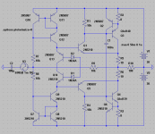
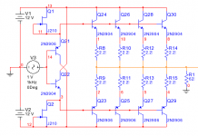
At any rate, here is my latest. For some reason it likes giving about 800mV pk-pk. It seems to me like its trying to turn 1mV to 1V, which would be a voltage gain of about 1k. R9 is feedback. The two germaniums can be replaced with a single silicon diode, but I was using them to test out the junction of the two bases as a possible feedback point. Both connections between Q13 and Q14 are candidates for feedback. Added Q2 and Q6 so that quiescent current cannot rise above about 75mA and so C1 won't crispy-fy the output pair. R1 and R4 are now 10k, which gives better OLG in the output drivers/pair, which also increases the effectiveness of the C1 coupling. R7 and R8 may be replaced with a trimmer with wiper to input so that output offset can be adjusted. However, this would also unevenly distribute signal between the output pair which would decrease maximum power output.
Next I'll experiment with higher input voltages and see what happens.
- keantoken
Attachments
go back to post 1 schematic. Start analysing that before you add any more complication.
Measure the voltage across R1 & R2. What value do you get?
These are the Vbe of Q3 & Q4.
Now what currents are flowing through Q1 & Q2? Are they equal?
what would be a better value for R1 & R2? Hint <100r.
Now, start looking at R5 & R7. Go on from there.
Next, R3 & R10.
You'll gather that I don't agree with any of the resistor values you have guessed at.
keantoken said:
At any rate, here is my latest. For some reason it likes giving about 800mV pk-pk. It seems to me like its trying to turn 1mV to 1V, which would be a voltage gain of about 1k. R9 is feedback. The two germaniums can be replaced with a single silicon diode, but I was using them to test out the junction of the two bases as a possible feedback point. Both connections between Q13 and Q14 are candidates for feedback.
Some possible problems:
* Q2/Q6, the short circuit protection transistors, will protect Q3/Q4 but will supply lots of current to turn Q1/Q5 into melted emitter followers. The short circuit protection should apply to the input of the CFP, which means it must crowbar in the other direction. R5/R6 are your overload sense resistors. See page 2 of the 741 datasheet, Q15 and Q21. Imagine that Q14 and Q20 are your CFPs.
* The OLG of the circuit is not well-controlled; it depends on (nonlinear) transistor characteristics. You need to have very predictable OLG/phase at high frequencies to ensure stability; this circuit is a discrete opamp. It looks like the + input is the junction of D1/D2 and the - input is the junction of R7/R8, but neither has very high input impedance. The gain from each input is different as well; the + input has unity gain, while the - input has higher gain (you claim 60dB).
Andrew:
Using your suggestions does help. However I am not sure why. It does make sense that running the drivers at higher current will increase their linearity, which I probably should have tried from the start. Right now I'm getting about 10mV of DC offset.
Sparcnut:
This is an amp, but not an entire one. This is just the output stage, the CAS. About short protection, I guess you are right. The bd139/140 have a max of 1.5A, I'll limit to 1.2A so .47 ohms for emitter resistors when I get to that point. Right now I'm waiting for Andrew to correct me again.
Thank you for your input.
- keantoken
Attachments
keantoken said:The bd139/140 have a max of 1.5A, I'll limit to 1.2A so .47 ohms for emitter resistors when I get to that point.
1.2A is way too much with 30V across them, check the SOA curves. 200mA is more like it, but they will still run warm (6W dissipation). The TO-92s you specify also are only rated for 50v, where in your circuit it is possible to swing nearly rail-to-rail (60v).
Carp. I don't know what else to use except the 2N3055/2955. :/
I'll try the MJL1302A/3281A. That's what Symasym uses.
EDIT: No... I can't get it to work... Why have I never found a good internet page on the workings of a CAS? Sheez, whenever I do figure it out I'm going to write a big wiki page on it.
- keantoken
I'll try the MJL1302A/3281A. That's what Symasym uses.
EDIT: No... I can't get it to work... Why have I never found a good internet page on the workings of a CAS? Sheez, whenever I do figure it out I'm going to write a big wiki page on it.
- keantoken
keantoken said:Carp. I don't know what else to use except the 2N3055/2955. :
I would use the BD139/140 at lower current and voltage (10mA/12v?), or some TO-92 devices at 1-5mA/12v. The smaller transistors can have far better high frequency characteristics, allowing much more HF gain in a circuit with NFB.
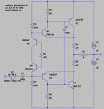
How about this?
I like the idea of using a bunch of small transistors to get decent wattage and nice characteristics.
I'll have to mess around and see if I can't get something to work... Currently I'm simming with LTSpice, but I'm wary since I've never heard of anyone getting Symasym to work on it.
- keantoken
I like the idea of using a bunch of small transistors to get decent wattage and nice characteristics.
I'll have to mess around and see if I can't get something to work... Currently I'm simming with LTSpice, but I'm wary since I've never heard of anyone getting Symasym to work on it.
- keantoken
Attachments
keantoken said:How about this?
That one might work for a little longer, but you are basically depending on Vbe of the output transistors matching. Unfortunately, Vbe in a bipolar has a negative temperature coefficient - as a transistor gets hotter, Vbe falls, and the current increases (due to the b-e junction being biased by a constant voltage by the rest of the circuit). Boom, thermal runaway.
I'm still not sure that the dual current mirror input stage is doing much good for you.
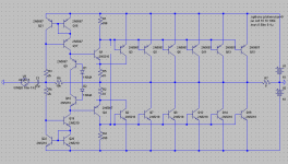
Edit - Here is a simple diamond buffer design that is pretty well-behaved. I have built this circuit several times, it works fine, free from thermal runaway/overload, stable, etc. Sounds very good. I drive 64-ohm headphones with it. Output transistor pairs can be removed if the extra power handling is not needed. The distortion performance of this circuit is decent: -90db 2nd harmonic, -100dB 3rd & others much lower using exactly the configuration shown. It can even be improved upon quite substantially with more components, but for simplicity I'm leaving it as-is for now. For my headphones, 4 output pairs is overkill (2 is enough, 1 would be fine on lower rails), but my whole philosophy for the rest of that amplifier was "total overkill" anyway
I use the "improved" version as the output stage of my discrete opamp for headphones; that design uses 38 TO-92 transistors per channel (!) but delivers better than -140dB distortion at 1KHz for typical levels (~80-90dB SPL on 64-ohm 102dB/mW 'phones). I have only simulated the distortion performance of that exact configuration, but Wednesday I should have a chance to drop it on an AP 2722 to see if it's true.
Attachments
- Status
- This old topic is closed. If you want to reopen this topic, contact a moderator using the "Report Post" button.
- Home
- Amplifiers
- Solid State
- Wait, do I finally understand the CAS?