Hi everyone,
Thank you for your answer on my previous topic about virtual ground / split supply. I really appreciate your help.
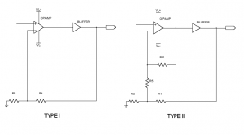
I have another one here. It's the feedback loop of the opamp + buffer normally used for the high current headphone amplifier.
From the buf634 and lm49600 datasheet they recommend type I schematic. however I have seen some design like type II so I would like to know if there is any benefit of doing this.
And also, if the gain of the buffer = 1, would it be better if I put it totally outside feedback loop?
Thank you in advance for your answer.")
Thank you for your answer on my previous topic about virtual ground / split supply. I really appreciate your help.
I have another one here. It's the feedback loop of the opamp + buffer normally used for the high current headphone amplifier.
From the buf634 and lm49600 datasheet they recommend type I schematic. however I have seen some design like type II so I would like to know if there is any benefit of doing this.
And also, if the gain of the buffer = 1, would it be better if I put it totally outside feedback loop?
Thank you in advance for your answer.
Attachments
type II is only needed if the buffer is a lot slower than the op amp. if you aqre using a buffer with the same or higher bandwidth buffer, use type I. go to www.linear.com and look up Application Note 47 for an in depth explanation of what happens with fast op amps and slow buffers.
LT's app note talks about that in detail. "overcompensating" a fast op amp to keep a slow buffer from oscillating. i had an idea for a power amp using an op amp as an input stage and a discrete VAS and output stage. the problem was that most of the op amps i tried caused oscillation. no amount of compensating the VAS could cure it, since the internal compensation of the op amp dominates the compensation of the whole amp. i finally "rolled my own" op amp so i could have control over the compensation, and other circuit parameters. i am currently redesigning the input stage again to include a method of adjusting open loop gain so i can have a variable output impedance.
I thought the idea with mulitloop, is to have just enough feedback in the "internal" loop to get a flat frequency curve in the audio spectrum (with some margins, like 100 kHz) for the opamp before global negative feedback is applied.
In the original article by Walt Jung, I think he used an AD823 as input stage and AD815 as buffer. AD815 is very much faster than AD823, so compensation for a low speed buffer can't have been the issue.
In the original article by Walt Jung, I think he used an AD823 as input stage and AD815 as buffer. AD815 is very much faster than AD823, so compensation for a low speed buffer can't have been the issue.
nelsonvandal said:I thought the idea with mulitloop, is to have just enough feedback in the "internal" loop to get a flat frequency curve in the audio spectrum (with some margins, like 100 kHz) for the opamp before global negative feedback is applied.
In the original article by Walt Jung, I think he used an AD823 as input stage and AD815 as buffer. AD815 is very much faster than AD823, so compensation for a low speed buffer can't have been the issue.
If the 2nd stage is just a buffer, there is no point in local feedback around it, as it has gain 1, so the interesting case is where the buffer also has gain (typically an op amp too). There are probably many good reasons for local feedback loops, but here are two:
1. Consider the simplified case of two identical single-pole op amps with open loop gain A and corner frequency f. A single such op amp has a unity gain frequency of Af and a a phase shift approaching 90 deg there. There is no problem at all with stability when applying feedback. Now cascade two such op amps. The composite open loop gain becomes A^2 (that is A*A). The corner frequency is the same, but since we now have a double pole there the unity gain frequency is still Af. However, because of the double pole we also approach 180 deg phase shift at unity gain, which can be troublesome when applying feedback. Then considering that real op amps have more than one pole, even if they are usually designed to have a strongly dominant one, means even more problem with phase shift. Using local feedback loops for the two op amps can give us more control over the phase shift.
2. The differential voltage at the input of an amp with feedback depends on the open loog gain of the amp. The higher the OLG, the lower the differential voltage. That is good for linearity, but bad for noise. If you cascade two open loop op amps and then apply feedback over both, you get a very low differential voltage at the first one, requiring a very-low-noise device. If we instead apply local feedback to both op amps, we get a higher differential voltage at the first one. That is, we get less noise, but loose some linearity.
Your point about getting a flatter frequency response may or may not be relevant depending on whether you think that matters or not. The most important thing is to have enough OLG at 20 kHz so feedback is effective. Some argue that it is also beneficial that the OLG is flat up to that point, but that is debated.
actually there is a purpose for including a buffer in a feedback loop. buffers are not completely distortion free, and including them in the feedback loop reduces any distortion that they might introduce in the system. remember, power amp output stages are buffers with unity voltage gain (in practice, just below unity, about 0.99) and tend to be slow buffers at that (with a power bandwidth below 1 Mhz in most cases). however, having a nested feedback loop can also have it's uses. the amp design i mentioned previously also suffered from poor clipping behavior. it would "hang" on the rails for about 50 microseconds, a sign something was saturating and not recovering immediately. when i used a nested feedback loop, limiting the op amp gain to 100, that cured the "hangover" problem (and i'm sure such clipping behavior would have caused a nasty headache after a few minutes of listening). since this amp will find some application as a guitar amp (guitar amps tend to spend a lot of time in their clipping region), the amp must clip as cleanly as possible.
Old thread, but I see Jed's still active. Thanks, that's a good find. Appendix C of AN47 was just what I was looking for.go to Linear Technology - Home Page and look up Application Note 47 for an in depth explanation of what happens with fast op amps and slow buffers.
I've long been aware of the difficulties the need for output power creates with PSRR a linearity at more typical listening levels but this LME49724+AD8017 composite amp I'm designing is doing an excellent job of educating me on bandwidth management. The 8017 should be good for 100MHz typ in the configuration I'm operating it in and the 49724 is 50MHz typ. Should be stable in most cases but looks marginal with a fast 49724 and a slow 8017. So the board has pads for comp caps. Walt Jung's articles have touched on the topic, as do the BUF634 and LMH6321 datasheets, and Jerald Graeme's op amp book has a chapter on it. But appendix C of AN47 is the best discussion on the topic I've come across so far. I only skimmed the rest of AN47 as it's largely material I'm already familiar with or out of scope to my present projects but it seems like a good introductory reference.
Some time ago I laid out a power amp board where an LME49990 controlled Sanken STD03N and STD03P output devices without any compensation. Probably a good thing I never sent it to fab as it looks like a stability trainwreck; 110MHz GBP op amp and BJTs where the transition frequency isn't even speced. It was never more than a 10W design anyway so it'd probably be happier implemented as an LME49710 using 2SA1859+2SC4883 with a comp cap.
Some time ago I laid out a power amp board where an LME49990 controlled Sanken STD03N and STD03P output devices without any compensation. Probably a good thing I never sent it to fab as it looks like a stability trainwreck; 110MHz GBP op amp and BJTs where the transition frequency isn't even speced. It was never more than a 10W design anyway so it'd probably be happier implemented as an LME49710 using 2SA1859+2SC4883 with a comp cap.
the discussion of Murphy's law in AN-47 is a must read.... the STD devices are the 5-pin Darlingtons, aren't they? compensation is a must when driving darlingtons, as they are notoriously slow, especially the prepackaged ones. at least with cascaded EF outputs you can select the drivers and output devices, but with the prepackaged darlingtons, you're stuck with whatever is in there..... there's a rule of thumb with japanese transistors 2SA, 2SC devices are faster than 2SB, 2SD devices. darlingtons tend to be in the 2SB, 2SD category
Last edited:
Arent most opamp buffers typical high gain opamps with a built in connection between out and -ve input (full negative feedback)? Draw the circuit including this buffer local feedback for a better idea of the circuit. This cant be considered equivalent to a power amp output stage?
I got curious and did a trawl through Sanken's lineup. The single emitter devices all have fTs of 20MHz and the slowest device in the LAPT pairings is typically 50MHz. The Darlingtons are mostly comparable to the LAPTs but the fastest pair of TO package power output devices Sanken makes is the 80MHz 2SB1559+2SD2389.compensation is a must when driving darlingtons as they are notoriously slow
This implies the STD01 and STD03 Darlingtons might be pretty quick---I have a bunch of STD03Ps I picked up for cheap; be interesting to measure some of them if I get around to it. In the meantime the 2SB1559 and 2SD2389 have a min hFE of 5000 so their bases are an easy load for an op amp. Likely wouldn't require too much compensation when used with something like an LME49710.
- Status
- This old topic is closed. If you want to reopen this topic, contact a moderator using the "Report Post" button.
- Home
- Amplifiers
- Solid State
- opamp + buffer feedback loop clarification