Have you read D.Joffe yet?
Have you read any of the many posts describing this dual channel input problem?
Do a search for D.Joffe to see how often it comes up. Search HBRR or HBRL.
That same search will show that I have posted the D.Joffe paper three times this year !!!!!!
Have you read any of the many posts describing this dual channel input problem?
Do a search for D.Joffe to see how often it comes up. Search HBRR or HBRL.
That same search will show that I have posted the D.Joffe paper three times this year !!!!!!
Now could you tell me where is the loop in my layout?
Here it is (see earlier posts in this thread):
Source --> L input GND --> L amplifier board --> power supply --> R amplifier board --> R input GND --> source.
This means that the "GND" of the source has two separate connections to your amplifier (GND wires of left and right RCA cables), which are then connected to each other again at the power supply "GND" of your amp. Voila, that's the loop! And the loop is broken once you disconnect one of the RCAs, exactly as you described it.
I believe I figured out the Joffe HBRR HBRL crypticism. The document about hum breaking resistors by David Joffe was surprisingly difficult to find.
ok
I have read the D.joffe documents.
He clarify the concept and talks about many kind of ground loop.
He suggests to insert HBRR/HBRL, but, in the pratice, my amp board doesn't have Signal GND and Power GND separated. They are put togeter in a star point on the board it self.
this is the pcb:
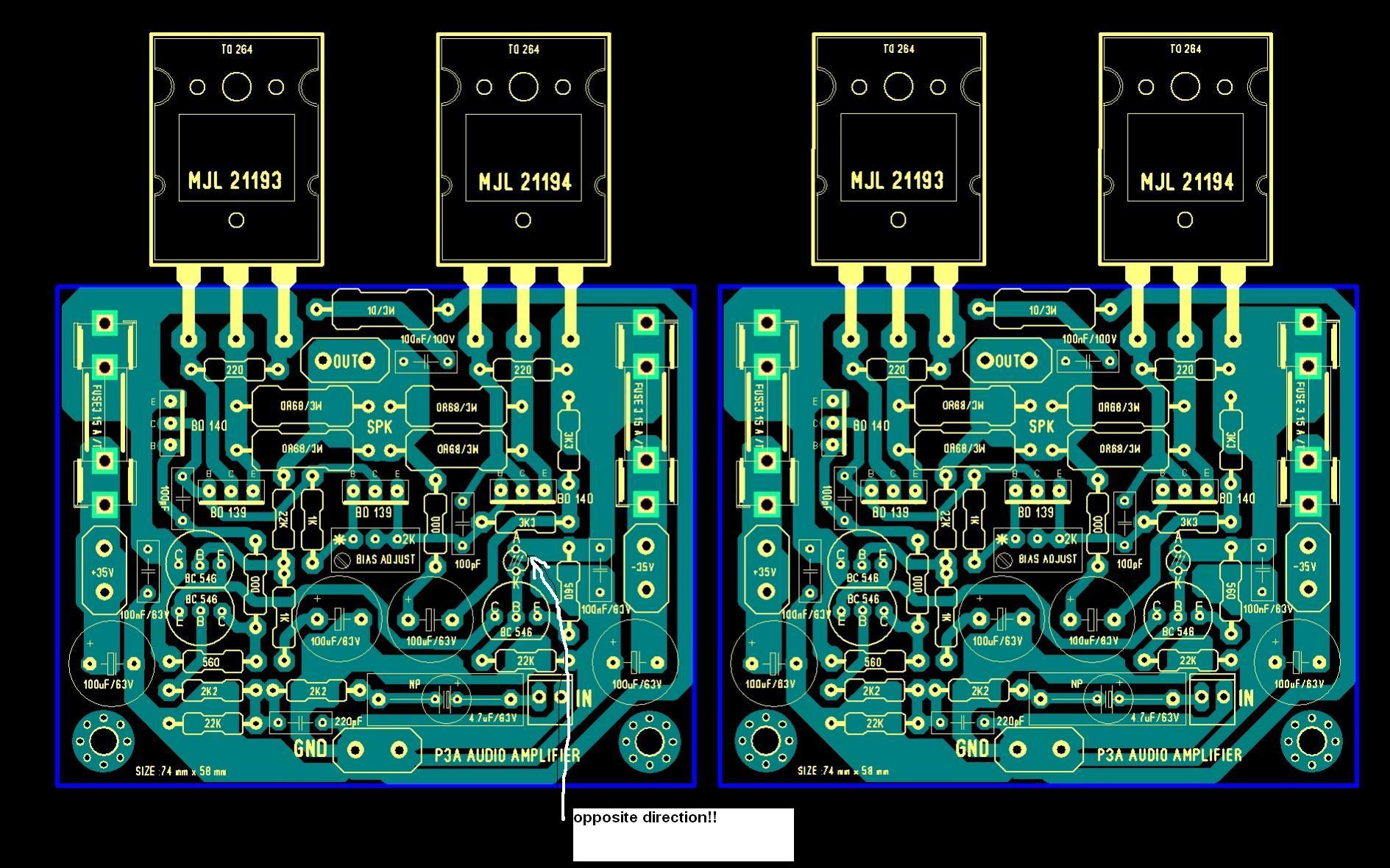
so where to put HBR?
I have read the D.joffe documents.
He clarify the concept and talks about many kind of ground loop.
He suggests to insert HBRR/HBRL, but, in the pratice, my amp board doesn't have Signal GND and Power GND separated. They are put togeter in a star point on the board it self.
this is the pcb:
so where to put HBR?
If you build a mono-block amplifier, then you can link the Signal Return to the Speaker Return and Power Ground without any "loop" consequences.
If you adopt any "joined" Signal and Speaker Returns PCB for a dual, or multichannel, amplifier then you will introduce a signal return loop where the source equipment has a commoned signal return for the two channels.
Building a multi-channel amplifier must either use a PCB that is suitable for multi-channel enclosures, or modify the PCB to make it suitable.
That means you find a PCB that has the Signal Return separated from the Speaker Return. Leach showed us this way back in his Lo Tim amplifier of the 1970s.
This separation was a feature in the modifications to the XY pcb Thread.
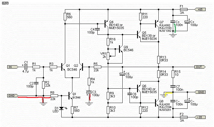
Start by looking at the schematic. Identify the Signal Return and what needs to be connected to it.
Identify the Speaker return and the Power Ground where the supply Rail decoupling meet up. What else needs to connect to that node?
Now separate these two nodes and use an added resistor as the voltage referencing link between the separated Returns.
Then see whether the PCB can be configured to match the modified SCH.
If you adopt any "joined" Signal and Speaker Returns PCB for a dual, or multichannel, amplifier then you will introduce a signal return loop where the source equipment has a commoned signal return for the two channels.
Building a multi-channel amplifier must either use a PCB that is suitable for multi-channel enclosures, or modify the PCB to make it suitable.
That means you find a PCB that has the Signal Return separated from the Speaker Return. Leach showed us this way back in his Lo Tim amplifier of the 1970s.
This separation was a feature in the modifications to the XY pcb Thread.
Start by looking at the schematic. Identify the Signal Return and what needs to be connected to it.
Identify the Speaker return and the Power Ground where the supply Rail decoupling meet up. What else needs to connect to that node?
Now separate these two nodes and use an added resistor as the voltage referencing link between the separated Returns.
Then see whether the PCB can be configured to match the modified SCH.
Last edited:

ok
in the pictures red traces are components that are in signal return path and they MUST be connected with it,
Yellow (better in pcb picture) is the route of main GND to the supply rail decoupling (at the end of each Yellow track we have a 100nf that connects gnd to V+ and gnd to V-)
can't draw speaker return because it is not on the board, it is a wire from spkr- to 0V on the psu or on the star ground.
is it correct?
ok I understand.the green Arrow is the position of 10ohm.
If I understand correctly, this resistor must be a sort of LINK between signal return and power gnd. So it needs the connections of the signal return must be left and untouched, we need to separate(cut) the union of the signal returns with the main ground but NOT the components that need to be linked to signal return path.
By now, a question: I have Elliot's original boards, and there is not any predisposition for this resistor, it means also that signal return is put together with main ground. So it will make an huum??????????
I suppose the level of interference will depend on how strong the emiis coming from other parts of the assembly and how big the loop area is of the input circuit.
If you can cut down the LOOP AREAS you will usually reduce the emi emitted and received.
After that is done by good layout, the remaining hum is attenuated by adopting the HBRR&HBRL resistors.
If you can cut down the LOOP AREAS you will usually reduce the emi emitted and received.
After that is done by good layout, the remaining hum is attenuated by adopting the HBRR&HBRL resistors.
Ok but this is possible also with my pcb!!!
I cant apply to my pcb cause i dont want to cut any track.
.i think there is simple way, a good way and the right way.
My layout is horrible, too many pcbs and long gng tracks in pcb...so high impedance and high noise to be picked up. I ll cure the layout with "t" system.
If it wont work anyway, i ll change project.
The Zobel on that PCB is useless, the long trace adds undesirable inductance and defeats the purpose of the Zobel. I could list down a few more issues, but will stick to the topic.
The PCB is designed to be used without the loop breaker and the signal, power and output returns are all at the tab at the lower edge of the board. Relocating the speaker return to the power supply increases the impedance of the input stage references and may cause some noise pickup. Usually you would crimp/solder the speaker return wire directly here.
In any case the decoupling currents are not properly separated from the low-level signal paths on this board, so some noise will intrude anyway. However, the kind of hum you mention seems to be classic ground loop issues caused by things like central power supply-based star ground schemes.
You have to remember that the interconnects also share a common 'ground' point, all the way to the power supply of the preamplifier or source or the output jacks (depending on topology, unless your source is a pure dual-mono construction as well).
When they meet again - regardless of where they meet, a resistive loop is formed that picks up interference from stray magnetic fields. This is usually injected straight into the input of the amplifier. The further away from the input circuitry the central ground reference is (impedance-wise) the worse the problem gets. The breaking circuits attempt to solve this problem by swamping any uncontrolled impedance with a much larger resistance, so the input and output currents get properly separated. This is slightly suboptimal as the best distortion performance is achieved with lowest possible return impedance, but it works reasonably well in most cases.
There are safety issues, as in the normal practice of isolating the RCA jacks from the chassis means that mains faults can cause dangerous voltages on them. The correct loop breaker circuit will also have diodes to keep the voltage across the circuit low, and a capacitor to counter the natural inductance of a low value resistor.
The chassis should obviously always connect to earth, no exceptions. If your binding posts are bare metal, the power supply common must also be connected to chassis either directly or through a disconnecting network. If a disconnecting network is used for the power common, you can directly connect the input and output references to a common node and there should be no noise. It looks like the PCB was designed for this kind of operation.
So in summary, looking at the diagram in post 4:
1. Disconnect the joints between the two RCA barrels and to any central points, if any - such as power supply board
2. Disconnect all speaker returns from the power supply
3. Throw away the central star
4. Connect power supply to the amp board using a three-wire connection. This is the only connection originating from the power supply board. The only exception would be a chassis connection - either direct or via network.
5. Connect binding post to the amplifier PCB using a two wire connection. One of these wires will connect to one of the wires mentioned in point 4) above, but ONLY at the amplifier PCB.
6. Connect RCA cable to the board using a two-wire connection, preferably twisted pair. The two connections of the RCA should connect to the two designated points on the PCB. Nowhere else.
7. Check for any noise. I wire most of my amps this way and have absolutely zero noise in the speaker at this point. However it can't be totally ruled out, sometimes the currents flowing in the PCB will continue to cause problems if it's not properly designed.
8. If at this point you get hum, insert the loop breaking resistors. You can do this by air-wiring the feedback cap negative, the 22k input biasing resistor and the 220pF cap together off the board, and connect it to either of the free pads using a 4-10 ohm resistor. The CCS biasing resistor can stay connected to power ground. Likely you should do it anyway, as the present layout mixes up low current and high current paths quite a bit.
Hi Sangram
Thanks for your reply . You are going to be very neat and clear in your explanation.
In reality, Im not a beginner")
I have been building amps for many years, but never built the p3a.
The issue is very common, and it is also simple to solve.
I THINK only you gave the correct answer somewhere in your post.
No cripticism or wisdom anyway, well done.
Very strange place diyaudio! Goodnight
Thanks for your reply . You are going to be very neat and clear in your explanation.
In reality, Im not a beginner
I have been building amps for many years, but never built the p3a.
The issue is very common, and it is also simple to solve.
I THINK only you gave the correct answer somewhere in your post.
No cripticism or wisdom anyway, well done.
Very strange place diyaudio! Goodnight
yes, I understand.
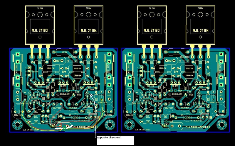
Right now, I'm gonna rebuilt it with a new layout...in your opinion, where I can make the ac wires from trafo to main plug pass through?
the route I think about should be the 2 lines in red, but it crosses the DC connection from CAPs to amp of the right channel. any suggestion?
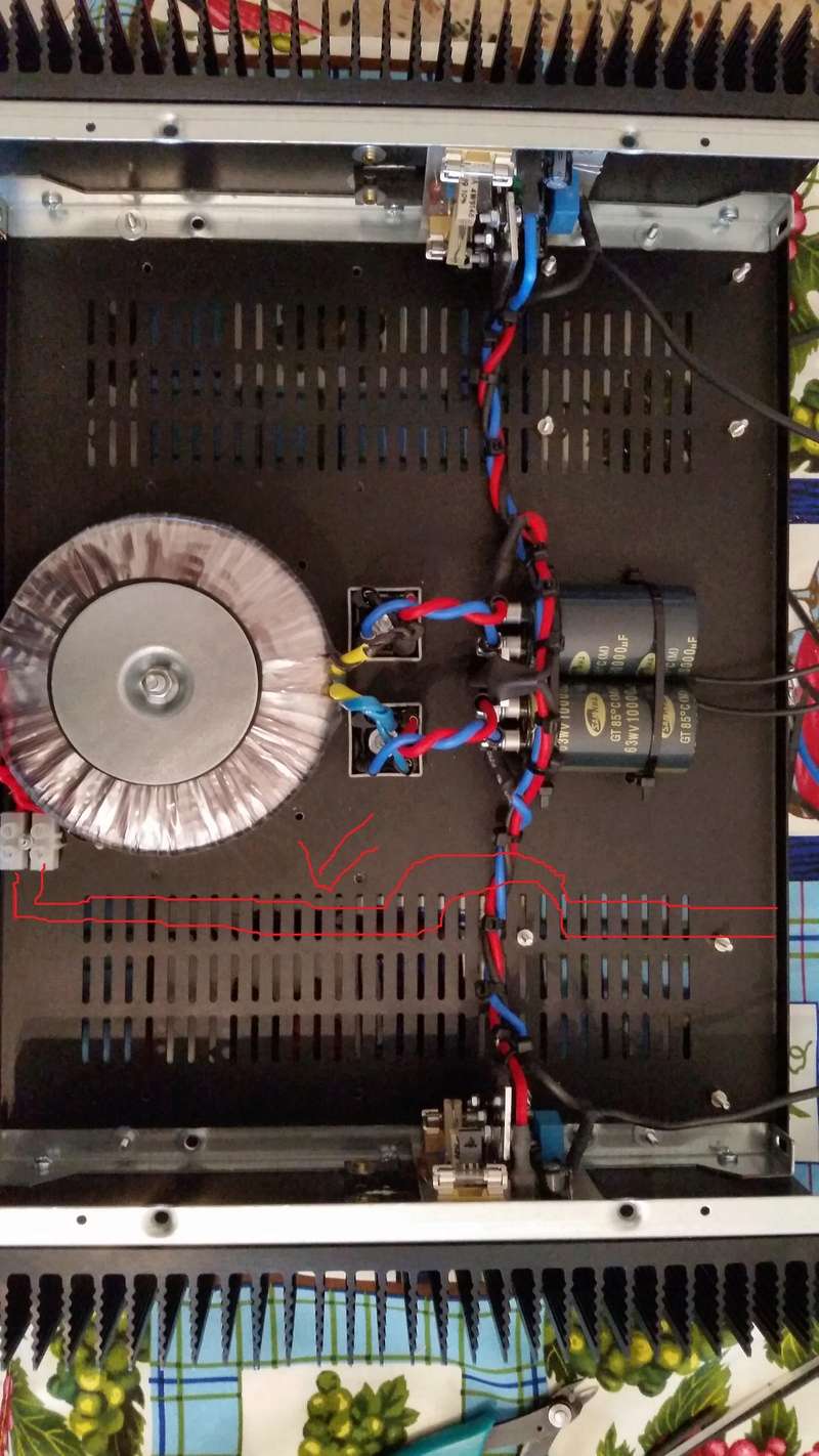
Right now, I'm gonna rebuilt it with a new layout...in your opinion, where I can make the ac wires from trafo to main plug pass through?
the route I think about should be the 2 lines in red, but it crosses the DC connection from CAPs to amp of the right channel. any suggestion?
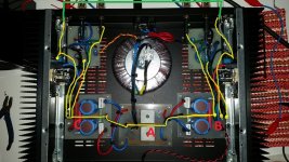
How it s made the T? How can i make it?
T is made of piece of copper. In my implementation I have connectors soldered to it in appropriate places, connecting all the ground wires, coming from the boards and plugs.
Initially, before I used the "T" approach, I had exactly the same issue - external loop through the cables. Now - no loop = dead silent amp with both channels connected to the source.
AndrewT is right with regards to "decoupling" resistor position. All the rest is fine.
This error disqualifies the article (upaded in december 2014) which relies on recommendations, not on explanations. Other points like isolated input and output sockets and one only chassis bond point can be contested. Better reference to more analytical articles.this Bonsai article has still not been corrected.
The "decoupling" resistor shown in the input wiring is inserted on the wrong side of the adjacent circuit node.
The resistor should be between the "Local Decoupling 0V" and the circuit node just to the left.
The Zobel on that PCB is useless, the long trace adds undesirable inductance and defeats the purpose of the Zobel. I could list down a few more issues, but will stick to the topic.
The PCB is designed to be used without the loop breaker and the signal, power and output returns are all at the tab at the lower edge of the board. Relocating the speaker return to the power supply increases the impedance of the input stage references and may cause some noise pickup. Usually you would crimp/solder the speaker return wire directly here.
In any case the decoupling currents are not properly separated from the low-level signal paths on this board, so some noise will intrude anyway. However, the kind of hum you mention seems to be classic ground loop issues caused by things like central power supply-based star ground schemes.
You have to remember that the interconnects also share a common 'ground' point, all the way to the power supply of the preamplifier or source or the output jacks (depending on topology, unless your source is a pure dual-mono construction as well).
When they meet again - regardless of where they meet, a resistive loop is formed that picks up interference from stray magnetic fields. This is usually injected straight into the input of the amplifier. The further away from the input circuitry the central ground reference is (impedance-wise) the worse the problem gets. The breaking circuits attempt to solve this problem by swamping any uncontrolled impedance with a much larger resistance, so the input and output currents get properly separated. This is slightly suboptimal as the best distortion performance is achieved with lowest possible return impedance, but it works reasonably well in most cases.
There are safety issues, as in the normal practice of isolating the RCA jacks from the chassis means that mains faults can cause dangerous voltages on them. The correct loop breaker circuit will also have diodes to keep the voltage across the circuit low, and a capacitor to counter the natural inductance of a low value resistor.
The chassis should obviously always connect to earth, no exceptions. If your binding posts are bare metal, the power supply common must also be connected to chassis either directly or through a disconnecting network. If a disconnecting network is used for the power common, you can directly connect the input and output references to a common node and there should be no noise. It looks like the PCB was designed for this kind of operation.
So in summary, looking at the diagram in post 4:
1. Disconnect the joints between the two RCA barrels and to any central points, if any - such as power supply board
2. Disconnect all speaker returns from the power supply
3. Throw away the central star
4. Connect power supply to the amp board using a three-wire connection. This is the only connection originating from the power supply board. The only exception would be a chassis connection - either direct or via network.
5. Connect binding post to the amplifier PCB using a two wire connection. One of these wires will connect to one of the wires mentioned in point 4) above, but ONLY at the amplifier PCB.
6. Connect RCA cable to the board using a two-wire connection, preferably twisted pair. The two connections of the RCA should connect to the two designated points on the PCB. Nowhere else.
7. Check for any noise. I wire most of my amps this way and have absolutely zero noise in the speaker at this point. However it can't be totally ruled out, sometimes the currents flowing in the PCB will continue to cause problems if it's not properly designed.
8. If at this point you get hum, insert the loop breaking resistors. You can do this by air-wiring the feedback cap negative, the 22k input biasing resistor and the 220pF cap together off the board, and connect it to either of the free pads using a 4-10 ohm resistor. The CCS biasing resistor can stay connected to power ground. Likely you should do it anyway, as the present layout mixes up low current and high current paths quite a bit.
pardon me if its bad to post on 2 year old post, as I'm stuck with same hum when 2 channels connected and more when with 5.1 setup.
Thankyou Sangram, if I dare say no one has explained it better on such issue, while many many people are facing cross channel loop, I am able to observe (can be my poor search) the same star ground reply, although its not solving results for man many threads, where either the novice poster get dis-heart or uses input line transformer.
(i am also facing looping hum via signal returns and seen few more threads tackling same thing over and over again)
The purpose of writing so much, if it can be made a sticky thread on this topic.
(I think i have seen that too, but very few talks about signal return loop and breaking resistor).
request to experts, kindly consider this cross channel looping too an issue, not everything can be only earth related (I hope many clueless noobs get direction from this)
Helpful read:
http://hifisonix.com/wordpress/wp-content/uploads/2018/07/How-to-wire-up-an-amplifier_2.pdf
Last edited:
- Status
- This old topic is closed. If you want to reopen this topic, contact a moderator using the "Report Post" button.
- Home
- Amplifiers
- Solid State
- Rod Elliot P3A amp noises