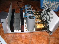
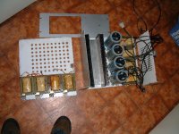
I've designed this amp some months ago, it worked well. The sound was good, but I still haven't finished the whole case (a little bit out of time and money).
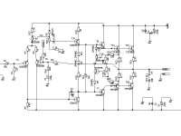
Attention! one transistor (T17) in the protection circuit is placed incorrect!! The pcb is correct! I've used other output transistors than shown in the schematic!! (BDV 66 - BDV67 I think) I've also experimented with the amount of bias diodes, the value of R28 and the adjustable CCS to get the right quiescent current.
Any comments are welcome.
best regards,
HB.
Attachments

Maybe pot R23 could have a zener from top to bottom so the voltage across it's length, and consequently the setting of ccs T14 won't vary with supply rail variations. The resistor below the pot that goes to 0v (can't see the schematic while replying!) may need to be lowered a bit.
My sugestions...
Hi hugobross!!!
Here is my sugestions:
-Change the Zener to two small sinal diodes (aka 1N4148) ...less noise!...as the LTP current is 2,5mA , R17 must be changed to 240 Ohm!
-Delete R 23 (pot) and conecte directely.the base of T14 to the diodes and the base of T13...then choose R 20 for 0'6 volts across it, with a current that you want for the Vas stage...after that, R1 must have a value to put +- 2 mA across the 4148 diodes...
The base of a CCS transistor like to see a stif voltage source at the base and the pot(R23) was kiling this!
- Put a 4'7 k resistor betwen the colector of T13 and the point of union of R7/R8...it will isolate the LTP from the nonlinear output capacitance of T13...
-Put a 100 Ohms resistor betwen the emitors of the drivers..
Tell me what you think!
Ps:some degeneration in the emitor of the lower Vas transistor (BD241 C) will be also a good idea..but R4 must be recalculated!
One more point...What is it for R 29 (22K)?
Thanks,
Circlotron, good point! What about placing a pot over the excisting zener??
Tube dude, I don't know if normal diodes have better noise figures than zeners; but I guess you're right! It's no big deal to change that!
I like this adjustable current source, and I'm not sure about deleting the pot.
A 100 ohm resistor between the driver emitters is a good idea
R29 is for bridging two of this amps, didn't use it by now.
euh, what do you mean with this one?? my english isn't that good I guess.
thanks,
HB.
Circlotron, good point! What about placing a pot over the excisting zener??
Tube dude, I don't know if normal diodes have better noise figures than zeners; but I guess you're right! It's no big deal to change that!
I like this adjustable current source, and I'm not sure about deleting the pot.
A 100 ohm resistor between the driver emitters is a good idea
In which way do you mean non-lineair?? I don't know if this non-lineair capacitance will affect the working of the LTP. The current through T13 is constant, right?- Put a 4'7 k resistor betwen the colector of T13 and the point of union of R7/R8...it will isolate the LTP from the nonlinear output capacitance of T13...
R29 is for bridging two of this amps, didn't use it by now.
Ps:some degeneration in the emitor of the lower Vas transistor (BD241 C) will be also a good idea..but R4 must be recalculated!
euh, what do you mean with this one?? my english isn't that good I guess.
thanks,
HB.
To Hugo...
zeners produce "white noise"...zeners are one of the elecronics components that produce more broadband noise...
The efect is even greater then when you take out the muting transistors in a CD player...the logical is about the same...and in a CD player the impedance is lower...the efect in the LTP is greater!!
To put a emiter resistor in this transistor(BD241C)....
Tube dude, I don't know if normal diodes have better noise figures than zeners
zeners produce "white noise"...zeners are one of the elecronics components that produce more broadband noise...
In which way do you mean non-lineair?? I don't know if this non-lineair capacitance will affect the working of the LTP. The current through T13 is constant, right?
The efect is even greater then when you take out the muting transistors in a CD player...the logical is about the same...and in a CD player the impedance is lower...the efect in the LTP is greater!!
euh, what do you mean with this one??
To put a emiter resistor in this transistor(BD241C)....
Looks good ")
Assuming you can't (or don't want to redesign the PCB ....
Don't you need a cut in the "ground loop" around the perimeter of the pcb?
Maybe I should rephrase that: I'd make a cut through that ring around the circuit.
Assuming you can't (or don't want to redesign the PCB ....
Don't you need a cut in the "ground loop" around the perimeter of the pcb?
Maybe I should rephrase that: I'd make a cut through that ring around the circuit.
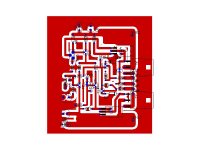
hugobross said:this was the first version of the pcb; this is incorrect! but it might be a good guideline to place the components.


This looks P3A derived.
Are the valus of R9 and R10 correct? I (mis-) calcvulate closed loop gain as:
G= (R9+R10)/R9 = (22,000+220)/220 = 101 ! This seems a tad high.
Other than cost, is there any advantage to the TIP3055/2955 pair over an sa1943/sc5200 pair? The latter have a higher fT and candle thermal and power with less effort.
sam9 said:
Other than cost, is there any advantage to the TIP3055/2955 pair over an sa1943/sc5200 pair?
probably not, I've used others too. Just stick in what you prefer most
Yes, maybe the gain is a little bit high, just increase the 220ohm resistor to reduce gain.
best regards,
HB.
The potentiometer connection, avoid! It is very sensitive to have a very important (and small) current only through the wiper of the pot. What happens if you get a bad contact with time? If you must have a trimming point there, just connect the potentiometer as a variable resistor.
Avoid as a general rule trimming of working conditions for the driver, not really necessary if the design is good.
I see that this trim potentiometer is for bias. You circuit has only -4.4 mV/C but you need at least 8.8 mV (you have 4 base-emitters). Risk for thermal runaway. Why don't you use a common Vbe multiplier? Easy, and works well.
Either I misread the schematic, or I don't understand it, or there is something wrong with the way the quiescent current is set.
If D8 is a 12V zener diode, there is always more than 11V across R20 and, hence, more than 11V across R28 since R28/R20=1. This would result in about 8A of quiescent current per output transistor, if it were not for the current limiting circuit, which limits the current to about 5A per output transistor. Is the current limiting circuit really intended to define the quiescent current? I'd guess this would give a rather nasty cross-over behaviour, with the output stage not responding at all to variations in T5's collector current until it enters a range where the current limiter doesn't work anymore.
Anyway, if the circuit is intended to operate as an ordinary class (A)B amplifier, I'd make the current source adjustable and proportional to the forward voltage across a bunch of diodes glued to the heat sink. For example, you could put two or three 1N4448's biased at a few milliamperes between the supply and the base of the current source transistor, and make its emitter resistor adjustable. Then put the 1N4448's and the transistor on the same heat sink as the output transistors and drivers. With 62 ohm for R28, the current source needs to supply about 20mA of current.
Further possible refinements in this case: connect a 150 ohm resistor between the emitters of T8 and T7 to make them operate in a non-switching manner, and then adjust the output stage quiescent current by adjusting the adjustable current source until there is 26mV across each output transistor emitter resistor. This should make the output stage operate near a distortion minimum.
Besides, you could try to come up with some kind of current limiting circuit for T5, because T5 and T17 may now be blown up when the output is short-circuited and the current limiting circuit switches on.
Finally, replacing R4 with a constant current source should give some distortion reduction, but keep in mind that you have only very limited voltage available for the current source. A small NPN transistor with its base biased at one diode forward voltage plus 300mV above the negative supply rail could just fit.
Just for fun I plugged the schematic in to a SPICE program. I use TIP31/32c's instead of BD240/241 because I had models available and they look to be pretty similar. I left the pot set at the midpoint which may be sub-optimal. The results were pretty good. A bit quieter than the P3A. The gain could be a problem in that it doesn't take much input voltage to drive the thing into clipping. To get normal usage out the volume control on the typical preamp, this power amp would probably benefit from it's own input attenuator/pot.
- Status
- This old topic is closed. If you want to reopen this topic, contact a moderator using the "Report Post" button.
- Home
- Amplifiers
- Solid State
- just found back a quick drawn schematic of my amp