Hi!
It has probably been discussed before, but if so, I couldn't find it.
Is it possible to bias the output stage in class A by referencing a current to the output node? If so, V+ or V-? Is it worth it sonically? Is the output stage class AB, and if so, which is the class A area currentwise, so a (very) light load resistor might work instead?
thank you,
Rüdiger
Onvinyl said:Hi!
Is the output stage class AB,
Quiescent current 8.2mA and +/-13v in 600ohm. Does it sound like class A?
")
What load do you have in mind?
Onvinyl said:Hi!
It has probably been discussed before, but if so, I couldn't find it.
Is it possible to bias the output stage in class A by referencing a current to the output node? If so, V+ or V-? Is it worth it sonically? Is the output stage class AB, and if so, which is the class A area currentwise, so a (very) light load resistor might work instead?
thank you,
Rüdiger
I don't know is it possible to bias AD797 in Class A I have never tried that mod, but if the answer is yes, you should always reference to -V, because you want to NPN output transistor to do the hard work, not PNP
Is it worth sonically?...Yes and no, you should try that for yourself, but be aware that the THD numbers will be up, but at the same time H2 will be up too, which can be pleasing to some ears.
Regarding standing current in AD797 output transistors, according to my simulation, it's about 0,5mA.
the datasheet claims 500uA output stage bias
push-pull operation operation means ~+/-1 mA load current would be delivered in Class A without additional bias, which turns out to be not much when using feedback impedance levels low enough to take advantage of the input noise performance
the AD797 has a unique local feedback option that essentially cancels the dominant pole compensation around the output stage local Cn loop, giving high loop gain for correction of output stage error:
http://www.diyaudio.com/forums/showthread.php?postid=1513928#post1513928
with the optimum Cn local feedback cap I doubt external Class A bias would give a measureable improvement
a possible difference between Class A and AB is that poor power supply routing could allow Class B rail currents to magnetically couple to low level signal loops - Self's "distortion #6:
http://www.dself.dsl.pipex.com/ampins/dipa/dipa.htm#2
I would suggest adding a buffer/gain stage with a CFA op amp in the feedback loop as shown in the datasheet fig 49 if ultimate low distortion performance was your goal
jcx said:the datasheet claims 500uA output stage bias
push-pull operation operation means ~+/-1 mA load current would be delivered in Class A without additional bias, which turns out to be not much when using feedback impedance levels low enough to take advantage of the input noise performance
the AD797 has a unique local feedback option that essentially cancels the dominant pole compensation around the output stage local Cn loop, giving high loop gain for correction of output stage error:
http://www.diyaudio.com/forums/showthread.php?postid=1513928#post1513928
with the optimum Cn local feedback cap I doubt external Class A bias would give a measureable improvement
a possible difference between Class A and AB is that poor power supply routing could allow Class B rail currents to magnetically couple to low level signal loops - Self's "distortion #6:
http://www.dself.dsl.pipex.com/ampins/dipa/dipa.htm#2
I would suggest adding a buffer/gain stage with a CFA op amp in the feedback loop as shown in the datasheet fig 49 if ultimate low distortion performance was your goal
This is correct, you rapidly get into touchy bypassing issues. You really have to think about where the harmonic energy in the supply current is going.
Is it possible to tap the signal from the decompensation pin 8 (point B in the simplified schematic) and connect it to a discrete output stage and wrap it in the feedback loop instead of the built in diamond buffer, just like you can from the compensation pin in AD829 and AD744?
Hi, JCX,
Is this applicable to power amp too? To make a better classB/AB output stage?with the optimum Cn local feedback cap I doubt external Class A bias would give a measureable improvement
To the output node via Cbc?You really have to think about where the harmonic energy in the supply current is going.
my sims with a ~500uA biased complementary follower added to my loop gain sim of the AD797 simplified schematic shows no difference in the IMD products with optimum Cn vs 15 mA ccs output bias for 20+21 KHz 1:1 with 10 mA peak output into the resistive load (feedback network) @11Vpk out 1KHz IMD is -120 dB with either approach
I don't believe that the output stage is the dominant distortion source in this example, I have found a "T" 2-pole compensation that in sim reduces the 1 KHz IMD to -126 dB, the compensation "coincidentally" shows peaking in the loop gain at 20 KHz – reducing the amplitude of the main signal components at all stages, both diff in v, and folded cascode i
rather than improving active device distortion performance it is possible that full Class A operation improves “parasitic” system level distortion mechanisms
when a Class AB stage drives a load with higher current than the Class A bias, then part of the time one output stage transistor is supplying all of the current from one supply V and the other is cut off, with the roles reversing for opposite signal polarity, this means the current in the power supply pins looks "half-wave rectified" - ie highly nonlinear
these nonlinear supply currents can cause nonlinear distortion in the amplifier/system even with perfect active device amplification - the nonlinear supply currents can couple inductively or through the return currents flowing in impedance in common with the signal
If the amp operates full Class A then the power supply currents are linear and parasitic coupling only slightly changes gain/frequency response and crosstalk without adding nonlinear distortion
I prefer a physically separate buffer/gain stage in the feedback loop to avoid loading and thermal feedback effects in the precision input op amp, the buffer stage could also be Class A to avoid the above"system parasitics" distortion mechanisms
In the case that the load is known and constant it is also possible to add a negative impedance amplifier in parallel with the precision op amp's output stage – I think this circuit was shown by Sandman – when the negative impedance matches the load impedance then most of the output current is supplied by the added negative impedance circuit's amplifier and the AD797 output wouldn't operate beyond it's +/- 1 mA Class A region – Sandman's circuit has the “advantage” of not adding “stages in series with the signal path” for those bent that way
About biasing monolithic opamps to class A. It's very easy to try with a resistor, CRD or JFET (maybe not as good as bipolar). I've done it a lot (not with AD797) and thought the world of it... until I tried it live - connecting/disconnecting it while playing. No bloody difference at all! It was all placebo.
BTW, what is the optimal implementation of AD797, resistor/capacitor values?
BTW, what is the optimal implementation of AD797, resistor/capacitor values?
Sorry, Mr.Higgins' main page says "Back Soon"
Reference:
The Design and Build of a Class ‘S’ Audio Amplifier. Matthew Higgins.
ES327: Third Year Project Final Report.
School of Engineering, University of Warwick, UK
If you PM me your email I could send you that paper (2.3MB)
- Klaus
Reference:
The Design and Build of a Class ‘S’ Audio Amplifier. Matthew Higgins.
ES327: Third Year Project Final Report.
School of Engineering, University of Warwick, UK
If you PM me your email I could send you that paper (2.3MB)
- Klaus
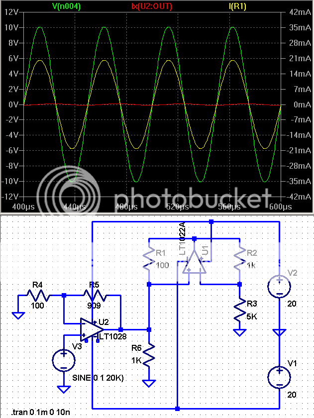
U2 is the precision amp, U1 is the cheap op amp negative impedance “buffer”
the combined load on U2 output is (R4+R5)||R6, where R4,5 are the feedback network and R6 is a load
R3 is a 10x scaled copy of the U2 load, the V across R2 might be thought of as measuring the current required to move R3 with the same V as the U2 load, R1 converts the measured voltage to a scaled current that just cancels the U2 load's current requirement – to the degree that R3 is an accurately scaled copy of the total load Z
U1 can be seen supplying nearly all of the load current in this sim through R1 (yellow)
U2 output current is ~260 uArms in this sim (red), mostly because at 20 Khz there is some phase lag in the synthesized negative impedance due to U1 GBW, a ~98% cancelation which should be better at lower frequencies - within the limits of component tolerances
nelsonvandal said:Is it possible to tap the signal from the decompensation pin 8 (point B in the simplified schematic) and connect it to a discrete output stage and wrap it in the feedback loop instead of the built in diamond buffer, just like you can from the compensation pin in AD829 and AD744?
This might be OK, but I'm not sure of the possible pitfalls.
There seems to be a lot of interest in this stuff I'm sorry I don't have more time to reopen the files.
- Status
- This old topic is closed. If you want to reopen this topic, contact a moderator using the "Report Post" button.
- Home
- Amplifiers
- Solid State
- Class A biasing for the AD797?