Having some problems with a new amp.
Any one any idea what causes this ?
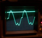
10KHz sine wave signal in.
Below 4 v pk 2 pk the output is fine.
Get above 4 v and the resulting waveform occurrs.
Have tried more drive current and it makes no difference.
Disconnected zobel network and again no difference.
Any input would be appreciated.
Nigel
Any one any idea what causes this ?
10KHz sine wave signal in.
Below 4 v pk 2 pk the output is fine.
Get above 4 v and the resulting waveform occurrs.
Have tried more drive current and it makes no difference.
Disconnected zobel network and again no difference.
Any input would be appreciated.
Nigel
Attachments
wg_ski said:That 100k limit sure makes schematics hard to read. This one takes the cake.
Cant be helped on a free site.........
The amp actually sounds fine which is odd !
If I hadnt seen the scope output I would have said it was OK.
An externally hosted image should be here but it was not working when we last tested it.
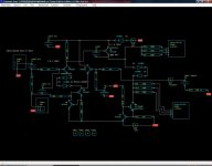
Heres a slightly bigger cct diagram
Hi
What does the square wave look like? Is there a difference between loaded and unloaded? I suspect it has something to do with the two diodes on the emitter of one transistor in the LTP and not the other. How is DC output? It should balance fairly close to 0VDC without these diodes. The bases of Q1 & Q2 should be the same voltage, at 0VDC, in order to have balance in the LTP. You must strive for current balance in the LTP.
You only have 2 diode drops as the gate spreader on the outputs? VgsTH is 2-4V for these devices. Could there be crossover noise since the outputs are in cut-off? These devices need thermal compensation as well. Look at the transfer characteristic curve (Fig 7) in the datasheet. See how Vgs decreases vs Id for an increase in temperature? It appears these devices have a positive temperature coefficient below 2A. If you bias at 2A, I guess you wouldn't need compensation, eh?
CBS240 said:Hi
What does the square wave look like? Is there a difference between loaded and unloaded? I suspect it has something to do with the two diodes on the emitter of one transistor in the LTP and not the other. How is DC output? It should balance fairly close to 0VDC without these diodes. The bases of Q1 & Q2 should be the same voltage, at 0VDC, in order to have balance in the LTP. You must strive for current balance in the LTP.
You only have 2 diode drops as the gate spreader on the outputs? VgsTH is 2-4V for these devices. Could there be crossover noise since the outputs are in cut-off? These devices need thermal compensation as well. Look at the transfer characteristic curve (Fig 7) in the datasheet. See how Vgs decreases vs Id for an increase in temperature? It appears these devices have a positive temperature coefficient below 2A. If you bias at 2A, I guess you wouldn't need compensation, eh?
If I unplug the speaker the signal is much more like a sine wave.
The 2 diodes on the LTP make the output close to zero volts, without them it can be close to a volt and the output transistors on one half run hot.
The 2 diodes used to bias the output rely more on negative feedback to get rid of crossover distortion. Any cutoff off period of both transistors will be minimal due to feedback compensating.
A square wave looks very rounded, I suspect due to the input filter.
What is odd it is only the negative half of the waveform with a problem.
On the previous smaller amp I built I just increased the drive to the output stage to get rid of a similar problem but that doesnt work this time. I am missing something somewhere.
Hi
Yes, the input filter will round the edges of the square wave and should be disconnected for that test. I suspect Q1 is under-biased with respect to Q2. Does the output look like this without those 2 diodes in the LTP even if it does produce DC? If the AC looks good, that may be where the problem is. If R5 is 120R then 5mA should flow evenly through Q1 & Q2. Ignoring the base current of Q5, to have 0.6V across R3 with 2.5mA is .6V/.0025A=240R. If the gain of MJE350 is 100 at 15mA, then current in R3 is 2.5mA less 150uA, or 2.35mA so 0.6V/.00235A=255R. I guess 260R would be closest real value. I can't read what the value for R3 is in the drawing.
Also, it sounds like the outputs are underbiased as well. The gates of the outputs should need about 6-7V between them for conduction.
CBS240 said:Hi
Yes, the input filter will round the edges of the square wave and should be disconnected for that test. I suspect Q1 is under-biased with respect to Q2. Does the output look like this without those 2 diodes in the LTP even if it does produce DC? If the AC looks good, that may be where the problem is. If R5 is 120R then 5mA should flow evenly through Q1 & Q2. Ignoring the base current of Q5, to have 0.6V across R3 with 2.5mA is .6V/.0025A=240R. If the gain of MJE350 is 100 at 15mA, then current in R3 is 2.5mA less 150uA, or 2.35mA so 0.6V/.00235A=255R. I guess 260R would be closest real value. I can't read what the value for R3 is in the drawing.
Also, it sounds like the outputs are underbiased as well. The gates of the outputs should need about 6-7V between them for conduction.
R3 is 12K.
Had a look at the output of the VAS and it looks very good.
So the distortion is coming after the MOSFETS. I am not sure why feedback doesnt correct the distorted signal.
I currrently have 20mA from a constant current source going through the VAS stage.
I upped the bias to 4.5 volts and it looks slightly different but not a lot.
I will probably have to investigate a proper bias cct.
you should have more bias on the FET gates, and you should have a 10uf or more cap across the bias stack. it looks like your output wave might actually be capacitive coupling of the drive signal through the gate capacitance, whuch would account for it collapsing with a load.
also you should get rid of D2. it doesn't seem to do anything but decrease your rail voltage by 0.7V.
i think your problem with the + half running warmer than the - side has a lot to do with the outputs being underbiased. and once you have proper bias, you might find that D2 and D5 aren't needed. without the bias you have a "dead zone" that the input stage must deal with by "finding" a stable operating point outside of the "dead zone".
unclejed613 said:you should have more bias on the FET gates, and you should have a 10uf or more cap across the bias stack. it looks like your output wave might actually be capacitive coupling of the drive signal through the gate capacitance, whuch would account for it collapsing with a load.
also you should get rid of D2. it doesn't seem to do anything but decrease your rail voltage by 0.7V.
i think your problem with the + half running warmer than the - side has a lot to do with the outputs being underbiased. and once you have proper bias, you might find that D2 and D5 aren't needed. without the bias you have a "dead zone" that the input stage must deal with by "finding" a stable operating point outside of the "dead zone".
Made the bias voltage about 5 volts and the distortion is starting to go.
I thought D2 decoupled the +ve supply from the driver stage ?
So noise on the PSU wont get into the driver stage?
Once the the 470uF is charged it cant discharge back through the diode........
It just seems odd the IRFP240 works fine on its on phase but the IRFP9240 has the distortion on its phase.
I guess once the IRFP9240 starts to go +ve again it has to discharge the inductor through the IRFP240. Maybe the dead zone is upsetting the IRFP9240?
I have designed a simple bias cct with a cap across it.
Will keep me busy tomorrow for a while.
Thanks for everyones input.
Regards Nigel
Nigel, there have been a few pointers in the previous responses, but I think there is a bit of cleaning up to do on this amp to get it performing well.
1. Remove th e LTP diodes. You are not getting to the root cause of your problem by inserting these.
2. The biggest problem here is the LTP load resistor of 12k. This is causing a massive imbalance in the LTP - 5uA is flowing on this side and 4.995mA on the other side and this is what is causing your distorted waveforms.
3. Insert 100 Ohm resistors in each LTP emitter
4. Change the LTP load resistor from 12 k to (0.8/2.5mA) = 320 Ohms - use 330 Ohms
5. Insert a small degen resistor between the emitter of the VAS transistor and the top rail. Calcualte from (0.8 - 0.6)/15mA = 13.3 Ohms - use 12 Ohms. The 15mA is your VAS standing current.
6. Reduce all those 47k Resistors - they are causing noise and uneccesary offsets. I'd bring the front end bias resistor down to 4k7 and reduce the feedback resistors to 4k7 and 100 Ohms.
7. Replace your feedback decoupling cap with something like 220uF 16V. This will give lower low frequenct distortion as well (see Self).
8.Dont forget your Zoebel (0.1uF in series with 10 Ohm) and an output inductor (2-5uH) with 2.2 Ohm in parallel
Once the above is done and your waveforms are cleaned up, you will ned to look into Cdom - if I read correctly this is 220pF - your should be able to reduce it drastically to improve slew rate performance and bandwidth
After this, next step will be to clean the output stage up. The bias voltage looks a bit low (2 Vbe?)
Good luck
")
1. Remove th e LTP diodes. You are not getting to the root cause of your problem by inserting these.
2. The biggest problem here is the LTP load resistor of 12k. This is causing a massive imbalance in the LTP - 5uA is flowing on this side and 4.995mA on the other side and this is what is causing your distorted waveforms.
3. Insert 100 Ohm resistors in each LTP emitter
4. Change the LTP load resistor from 12 k to (0.8/2.5mA) = 320 Ohms - use 330 Ohms
5. Insert a small degen resistor between the emitter of the VAS transistor and the top rail. Calcualte from (0.8 - 0.6)/15mA = 13.3 Ohms - use 12 Ohms. The 15mA is your VAS standing current.
6. Reduce all those 47k Resistors - they are causing noise and uneccesary offsets. I'd bring the front end bias resistor down to 4k7 and reduce the feedback resistors to 4k7 and 100 Ohms.
7. Replace your feedback decoupling cap with something like 220uF 16V. This will give lower low frequenct distortion as well (see Self).
8.Dont forget your Zoebel (0.1uF in series with 10 Ohm) and an output inductor (2-5uH) with 2.2 Ohm in parallel
Once the above is done and your waveforms are cleaned up, you will ned to look into Cdom - if I read correctly this is 220pF - your should be able to reduce it drastically to improve slew rate performance and bandwidth
After this, next step will be to clean the output stage up. The bias voltage looks a bit low (2 Vbe?)
Good luck
Hi
OK. This means that Vbe of Q5, 0.6V, is across R3. 0.6V/12K is 50uA. So Ic in Q1 is 50uA + 200uA (base current of Q5 @ 20mA) = 250uA. This leaves 5mA-0.25mA=4.75mA of Ic for Q2....hardly balanced.
Feedback does not correct errors, but rather modulates them with the input signal. This doesn't necessary equal a corrected signal at the output. Having a linear open loop gain is important for precisely this reason. Crossover distortion contains high frequency components. If these harmonics are higher than the OL bandwidth of the amp, feedback will have little effect.
Refer to the datasheet as to the Vgs threshold voltage. Better yet, measure it. You will probably find it about 3-3.5V. Since this is for each device, you will need at least 6-7V. Once you have them conducting 100-200mA, a more respectable bias, you may find the current will drift higher as they get hotter. I would suggest a Vgs multiplier cct to counter this effect. There is lots of info on this cct in the forum. What is the value of the source resistors on your output transistors?
Oh yeah.....and do what Bonsai suggested, you will have better results.
R3 is 12K.
OK. This means that Vbe of Q5, 0.6V, is across R3. 0.6V/12K is 50uA. So Ic in Q1 is 50uA + 200uA (base current of Q5 @ 20mA) = 250uA. This leaves 5mA-0.25mA=4.75mA of Ic for Q2....hardly balanced.
Had a look at the output of the VAS and it looks very good.
So the distortion is coming after the MOSFETS. I am not sure why feedback doesn’t correct the distorted signal.
Feedback does not correct errors, but rather modulates them with the input signal. This doesn't necessary equal a corrected signal at the output. Having a linear open loop gain is important for precisely this reason. Crossover distortion contains high frequency components. If these harmonics are higher than the OL bandwidth of the amp, feedback will have little effect.
I upped the bias to 4.5 volts and it looks slightly different but not a lot.
I will probably have to investigate a proper bias cct.
Refer to the datasheet as to the Vgs threshold voltage. Better yet, measure it. You will probably find it about 3-3.5V. Since this is for each device, you will need at least 6-7V. Once you have them conducting 100-200mA, a more respectable bias, you may find the current will drift higher as they get hotter. I would suggest a Vgs multiplier cct to counter this effect. There is lots of info on this cct in the forum. What is the value of the source resistors on your output transistors?
Oh yeah.....and do what Bonsai suggested, you will have better results.
wg_ski said:That 100k limit sure makes schematics hard to read. This one takes the cake.
I find it's mostly the daft image size (hor. and vert. pixels) constraint that hinders things.
If you save a schematic as a monochrome .jpg or .gif 100k is more than enough.
For example, this unattachable file is only 39k:
http://users.picknowl.com.au/~glenk/K10ASCH.GIF
I can understand putting a cap on the file size due to storage limitations, but the image size???????????
Cheers,
Glen
Hi Bonsai
Not really intended as a 'correction' per say, I just wanted to point out, other than the gross mis-balance of LTP current , that with MJE350 beta at about 100 for that current range (as per the datasheet ), base current can't be completely ignored. A buffered VAS would make the VAS base current more or less negligible from the POV of the LTP, which is an advantage. The suggestions you made are a good place to start. The circuit could be improved from there, but only by the subject comprehension of the builder, IMO.
 This is a hobby for me, but I have made circuits similar to this in the past. I’ve learned improvements may be rewarding but remain meaningless unless you know why they are improvements. That's where it begins to get technical...
Not really intended as a 'correction' per say, I just wanted to point out, other than the gross mis-balance of LTP current
, that with MJE350 beta at about 100 for that current range (as per the datasheet ), base current can't be completely ignored. A buffered VAS would make the VAS base current more or less negligible from the POV of the LTP, which is an advantage. The suggestions you made are a good place to start. The circuit could be improved from there, but only by the subject comprehension of the builder, IMO. This is a hobby for me, but I have made circuits similar to this in the past. I’ve learned improvements may be rewarding but remain meaningless unless you know why they are improvements. That's where it begins to get technical...CBS240 said:Hi
OK. This means that Vbe of Q5, 0.6V, is across R3. 0.6V/12K is 50uA. So Ic in Q1 is 50uA + 200uA (base current of Q5 @ 20mA) = 250uA. This leaves 5mA-0.25mA=4.75mA of Ic for Q2....hardly balanced.
Feedback does not correct errors, but rather modulates them with the input signal. This doesn't necessary equal a corrected signal at the output. Having a linear open loop gain is important for precisely this reason. Crossover distortion contains high frequency components. If these harmonics are higher than the OL bandwidth of the amp, feedback will have little effect.
Refer to the datasheet as to the Vgs threshold voltage. Better yet, measure it. You will probably find it about 3-3.5V. Since this is for each device, you will need at least 6-7V. Once you have them conducting 100-200mA, a more respectable bias, you may find the current will drift higher as they get hotter. I would suggest a Vgs multiplier cct to counter this effect. There is lots of info on this cct in the forum. What is the value of the source resistors on your output transistors?
Oh yeah.....and do what Bonsai suggested, you will have better results.
The source resistors are 0R22.
With 0.22 Ohms, 150mA would be 33mV across each one. So 30-40mV should be a good range for DC bias in the outputs.
I agree. Since they make both polarities of transistors, IMO complementary symmetrical is the way to go. The bridge amp circuit I'm working on, is for the most part completely designed. It's just the budget allocated for this 'not so cheap' hobby hasn't been up to the challenge. Things may start to happen soon though. 
Bonsai said:...the Self blameless topology is not really my cup of sake - I prefer fully balanced. [/B]
I agree. Since they make both polarities of transistors, IMO complementary symmetrical is the way to go. The bridge amp circuit I'm working on, is for the most part completely designed. It's just the budget allocated for this 'not so cheap' hobby hasn't been up to the challenge.
Things may start to happen soon though. CBS240 said:Hi
OK. This means that Vbe of Q5, 0.6V, is across R3. 0.6V/12K is 50uA. So Ic in Q1 is 50uA + 200uA (base current of Q5 @ 20mA) = 250uA. This leaves 5mA-0.25mA=4.75mA of Ic for Q2....hardly balanced.
Feedback does not correct errors, but rather modulates them with the input signal. This doesn't necessary equal a corrected signal at the output. Having a linear open loop gain is important for precisely this reason. Crossover distortion contains high frequency components. If these harmonics are higher than the OL bandwidth of the amp, feedback will have little effect.
Refer to the datasheet as to the Vgs threshold voltage. Better yet, measure it. You will probably find it about 3-3.5V. Since this is for each device, you will need at least 6-7V. Once you have them conducting 100-200mA, a more respectable bias, you may find the current will drift higher as they get hotter. I would suggest a Vgs multiplier cct to counter this effect. There is lots of info on this cct in the forum. What is the value of the source resistors on your output transistors?
Oh yeah.....and do what Bonsai suggested, you will have better results.
Added a better VAS cct tonight, around 5v5 the distortion goes.
I put in low ampage fuses to check the cct.
Blew 2 sets of fuses setting up the VAS so a bit wary now of VAS ccts ! The amp seems to be fine now.
Many thanks to all who contributed.
Nigel
- Status
- This old topic is closed. If you want to reopen this topic, contact a moderator using the "Report Post" button.
- Home
- Amplifiers
- Solid State
- AMP problem