Hi, I am trying to understand the popular symasym 5.3 audio amplifier because I think it is a good example to start with..
I'm currently analyzing the input stage and have a few doubts, please help if you can:
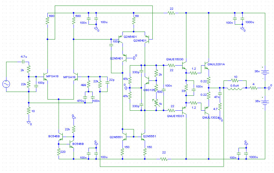
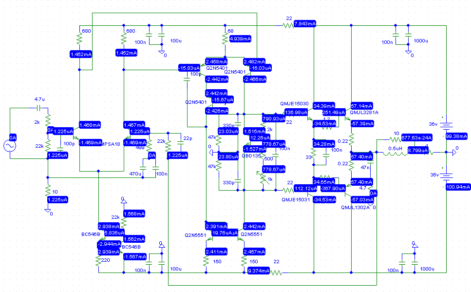
Ok so this is for the INPUT STAGE:
- Calculating the current of the BJT current sink give a value of about 3mA. This current then separates in half to bias the MPSA18 BJTs, but here comes the part i don't understand, shouldn't the collectors DC voltage be set near 0v to allow maximum possible swing? With this small current the collectors sit on vdd and have no swing at all. The collector resistors should be of a higher resistance?
- The differential gain i calculated is Avd=-gm*Rc=-0.0592*(680+22*2)=-43 But in multisim(with the weird dc value) give a gain of about -14. I also note that the output is a distorted sinusoid, because of the swing difficulties?
- What is the 10 Ohm resistor for? Why doesn't it connect directly to ground?
- What are all those resistors in the BJTs bases for? Couldn't one connect the input directly to the transistors bases because is would help CMRR? By my calculations :
Left BJT:
- The 4.7uF capacitor implements a high pass filter with fc=1.41Hz
- 100pF low pass 868Khz
Right BJT:
- 470uF low pass 0.34Hz!
- 100n low pass but when in comes into consideration the 470uF capacitor is shorting it, 470uF is more like a resistor in high frequencies?
- The 22kOhm implements a feedback loop?
I hope my English is understandable enough, sorry about that.
Thanks.
I'm currently analyzing the input stage and have a few doubts, please help if you can:
Ok so this is for the INPUT STAGE:
- Calculating the current of the BJT current sink give a value of about 3mA. This current then separates in half to bias the MPSA18 BJTs, but here comes the part i don't understand, shouldn't the collectors DC voltage be set near 0v to allow maximum possible swing? With this small current the collectors sit on vdd and have no swing at all. The collector resistors should be of a higher resistance?
- The differential gain i calculated is Avd=-gm*Rc=-0.0592*(680+22*2)=-43 But in multisim(with the weird dc value) give a gain of about -14. I also note that the output is a distorted sinusoid, because of the swing difficulties?
- What is the 10 Ohm resistor for? Why doesn't it connect directly to ground?
- What are all those resistors in the BJTs bases for? Couldn't one connect the input directly to the transistors bases because is would help CMRR? By my calculations :
Left BJT:
- The 4.7uF capacitor implements a high pass filter with fc=1.41Hz
- 100pF low pass 868Khz
Right BJT:
- 470uF low pass 0.34Hz!
- 100n low pass but when in comes into consideration the 470uF capacitor is shorting it, 470uF is more like a resistor in high frequencies?
- The 22kOhm implements a feedback loop?
I hope my English is understandable enough, sorry about that.
Thanks.
These pictures are from the symasym5 project page http://www.lf-pro.net/mbittner/Sym5_Webpage/symasym5_3.html
Answering yr questions
I think you should direct these questions to M. Bittner himself, he would be able to answer them promptly.
I am able to answer one question, ie the 10ohm resistor, you will note that the o/p gnd is connected directly to 0 V and the i/p gnd is via 10ohm, this because the you want to isolate the "noisy" o/p gnd from the "quiet" i/p gnd via a small resistor, anything close to 10ohm is adequate. This technique was used many years ago that I can remember, say >30yrs. I built an amplifier which used this technique, built 30 yrs ago!
The reason the collectors of your input pair stay close to the rail voltage is because they are clamped to that voltage via the Vbe drop (the diode between the base and the emitter) of the next stages PNP transistors whos emitters are tied to the plus rail through the 68 ohm resistor. The Q2N5401 transistors get the base current sourced through them and amplify it (Ic = Ib * beta). there are many reasons for adding input resistors to transistors, for the input pair it is more than likely it was to increase the input resistance as well as making a low pass filter.
serj,
The differential gain of a differential stage is approximately
Gain=gm*Rc
where gm=40*Ic at 25 degrees C.
So you equation is somewhat correct, but where did you get the 2*22? In addition, the loading of the second stage must be considered. The input resistance of the second stage is approximately Rin=2*Hfe/gm. This resistance must be included in the value for Rc. 1/2 of Rin must be put in parallel with each collector resistor.
I don't know what the 10 ohm resistor is used for, but it won't have much effect at audio frequencies.
The 4.7 uF cap is just for DC blocking. The 100 pF is a noise filter.
The 470 uF cap is just for DC coupling. It could be smaller, but you don't want it to effect the low frequency performance. The 100 nF would not be necessary except for high frequencies. The ESR of the 470 uF cap could be fairly large.
The 22K feedback resistor along with the 499 ohm resistor sets the gain.
Rick
O consulted Douglas Self's book but he doesn't go into much circuit analysis, i think it's a little more advanced. But i will look for Randy Slone's book if i can find it thank you.Andy L. Francis said:Let's read the primal Symasym thread regularly, and study Randy Slone's and/or Douglas Self's book(s)!
sawreyrw said:serj,
The differential gain of a differential stage is approximately
Gain=gm*Rc
where gm=40*Ic at 25 degrees C.
So you equation is somewhat correct, but where did you get the 2*22? In addition, the loading of the second stage must be considered. The input resistance of the second stage is approximately Rin=2*Hfe/gm. This resistance must be included in the value for Rc. 1/2 of Rin must be put in parallel with each collector resistor.
I don't know what the 10 ohm resistor is used for, but it won't have much effect at audio frequencies.
The 4.7 uF cap is just for DC blocking. The 100 pF is a noise filter.
The 470 uF cap is just for DC coupling. It could be smaller, but you don't want it to effect the low frequency performance. The 100 nF would not be necessary except for high frequencies. The ESR of the 470 uF cap could be fairly large.
The 22K feedback resistor along with the 499 ohm resistor sets the gain.
Rick
Hi sawreyrw. I got the 2*22 because i think since the currents from the collectors join in the 22Ohm they see efectively double the resistance, at least this is how it works for the resistor in the emitters.
I think you can ignore the input resistance of the second stage because it must be much larger than 680Ohm.
Thanks all
") I'll try to wrap things up and analyse he rest of the circuit soon.
I'll try to wrap things up and analyse he rest of the circuit soon.If I might break in...
What is the benefit of the part of the circuit I have circled below? If I understand correctly, Cdom is here, rather than on the VAS?
The reason I ask is because in my simulation of this amp, this seems to cause a lot of instability, especially evident at the base of the VAS.
Please excuse my ignorance, I'm just trying to understand.
Attachments
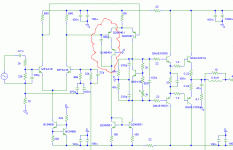
It looks to me like Cdom was placed there to help increase slew rate. by placing it there you would not have to sink and source additional current to it from the VAS, but rather the other side of the current mirror. I have seen other amps that include Cdom placed so that it incorporates the entire output stage just for that reason.
AndrewT said:The Cdom sinks and sources current from the LTP.
That's what's problematic with the conventional Cdom/Miller comp cap location.
AndrewT, you are correct. I misspoke in my explanation. It sounded much clearer in my head but did not come out right. If you look at it from an open loop stand point, there are no low AC impedances between the LTP and the VAS, and all of the current from the LTP is sunk through the gain transistor, giving better rise time. I was trying to say that the current mirror isolates them. By closing the loop the feedback loop side is sinking and sourcing the additional current need by the miller cap. But I would tend to think that this method would render the feedback path less effective for high frequency feedback.
After playing around with this amp in multisim for alittle while I have found that by placing the miller cap in it's current position the amp does indeed acquire a faster slew rate. In it's current position, the amp achieves a slew rate of about 8.5V/us. If it is moved to the other side (between the base and collector) of the VAS transistor, it achieves a slew rate of 5.97V/us. The other interesting notes are that the THD is reduced by a fair amount by keeping it were it currently is, this is probably no doubt due to the reduced ac load on the LTP. A couple of other interesting tide bits are that the miller cap does slow down the feedback loop causing gain peaking at around 1Mhz, but this only happens if the 22pF cap in the feedback loop is removed, this is acting as a high frequency bypass to help the feedback loop keep linear at high frequency response. I can post the Bode plots if anyone would like.
Well,
LTP gain
Ku=Rc/re
     Rc=680||Rin
     Rin=The input resistance of the second stage.
     Rin=3K
     Rc=680||3K=554Ohm
     re=26mV/Ic=26mV/1.5mA=17ohm.
ku=554/17=32.5V/V (for symmetric output)
And 16V/V for asymmetric output.
I ignore H22 (gce) in gain calculation.

VAS gain is approximately equal
ku2=Rc/re
   Rc=(rce/2)||Rin output stage=20K||20k=10K
   Rin=hfeUs5*hfeUs3*Rl=100*50*4=20K
   rce=1/H22=100V/Ic=40K
   re=10 ohm
   ku2=20K/10=1K [V/V]
Open loop gain is 1K*32=32000=32K
Close loop gain is
KUf=1+(R29/R30)=1+(22K/509)=43[V/V]=32dB.

Input impedance of amplifies equal R14=22K.

Left BJT:
- The 4.7uF capacitor implements a high pass filter
Fc=0.16/(C*R)=0.16/(4.7uF*23K)=1.4Hz
- 100pF low pass whit 2K
Fc=0.16/(100pF*2K)=800KHz

Right BJT:
- 470uF high pass
Fc=0.16/(470uF*509)=0.6Hz
22p low pass
Fc=0.16/(22p*22K)=330KHz
That how I see this
LTP gain
Ku=Rc/re
Rc=680||Rin
Rin=The input resistance of the second stage.
Rin=3K
Rc=680||3K=554Ohm
re=26mV/Ic=26mV/1.5mA=17ohm.
ku=554/17=32.5V/V (for symmetric output)
And 16V/V for asymmetric output.
I ignore H22 (gce) in gain calculation.
VAS gain is approximately equal
ku2=Rc/re
Rc=(rce/2)||Rin output stage=20K||20k=10K
Rin=hfeUs5*hfeUs3*Rl=100*50*4=20K
rce=1/H22=100V/Ic=40K
re=10 ohm
ku2=20K/10=1K [V/V]
Open loop gain is 1K*32=32000=32K
Close loop gain is
KUf=1+(R29/R30)=1+(22K/509)=43[V/V]=32dB.
Input impedance of amplifies equal R14=22K.
Left BJT:
- The 4.7uF capacitor implements a high pass filter
Fc=0.16/(C*R)=0.16/(4.7uF*23K)=1.4Hz
- 100pF low pass whit 2K
Fc=0.16/(100pF*2K)=800KHz
Right BJT:
- 470uF high pass
Fc=0.16/(470uF*509)=0.6Hz
22p low pass
Fc=0.16/(22p*22K)=330KHz
That how I see this
Thanks jony!
I wrapped your post in CODE tage to keep spaces. I think Rin of output stage is only 10K because in AC, output transistor is parallel to each other
I wrapped your post in CODE tage to keep spaces. I think Rin of output stage is only 10K because in AC, output transistor is parallel to each other
Code:
Well,
LTP gain
Ku=Rc/re
Rc=680||Rin
Rin=The input resistance of the second stage.
Rin=3K
Rc=680||3K=554Ohm
re=26mV/Ic=26mV/1.5mA=17ohm.
ku=554/17=32.5V/V (for symmetric output)
And 16V/V for asymmetric output.
I ignore H22 (gce) in gain calculation.
VAS gain is approximately equal
ku2=Rc/re
Rc=(rce/2)||Rin output stage=20K||20k=10K
Rin=hfeUs5*hfeUs3*Rl=100*50*4=20K
rce=1/H22=100V/Ic=40K
re=10 ohm
ku2=20K/10=1K [V/V]
Open loop gain is 1K*32=32000=32K
Close loop gain is
KUf=1+(R29/R30)=1+(22K/509)=43[V/V]=32dB.
Input impedance of amplifies equal R14=22K.
Left BJT:
- The 4.7uF capacitor implements a high pass filter
Fc=0.16/(C*R)=0.16/(4.7uF*23K)=1.4Hz
- 100pF low pass whit 2K
Fc=0.16/(100pF*2K)=800KHz
Right BJT:
- 470uF high pass
Fc=0.16/(470uF*509)=0.6Hz
22p low pass
Fc=0.16/(22p*22K)=330KHz
That how I see this- Status
- This old topic is closed. If you want to reopen this topic, contact a moderator using the "Report Post" button.
- Home
- Amplifiers
- Solid State
- Beginner symasym circuit analysis