http://www-f9.ijs.si/~margan/Articles/Class_B_Dist.pdf
Hi,
Anyone know anything about :
References
1. E. Margan, Add-on current dumping,
Electronics & Wireless World, 1985, October,
p.40.
Referred to in the above article ?
is it really non switching class B ?
Is there a good explanation of it anywhere ? (I cannot find any info).
How does S2 in figure 2 work ?
it looks like it will blow the amplifier up ........
") /sreten.
/sreten.
Hi,
Anyone know anything about :
References
1. E. Margan, Add-on current dumping,
Electronics & Wireless World, 1985, October,
p.40.
Referred to in the above article ?
is it really non switching class B ?
Is there a good explanation of it anywhere ? (I cannot find any info).
How does S2 in figure 2 work ?
it looks like it will blow the amplifier up ........
/sreten.The idea behind is seems to be the following:sreten said:is it really non switching class B ?
Is there a good explanation of it anywhere ? (I cannot find any info).
Basically the output is an emitter follower in a CFP-like configuration. Under normal conditions the current sense circuitry around the top and bottom 0.4R resistors is off (the transistors are off). When the current starts to cease as the output current increases for the opposite side, the voltage increases across the sense transistor's Vbe junction, starting to turn it on (the diode provides a bias point for this). This in turn spreads the bias (as established by the primary bias circuit) due to voltage drop on the 200R base resistor which now gets pulled towards the rail. Which increases current up to an equilibrium point, a feedback loop in the end. Therefore the outputs never turn completly off.
You might want to check out the LT1166 bias generator, which does more or less the same thing but a bit more clever, without the additional sense resistors, using the drop across emitter resistors directly.
If it's a bad design, it will. Otherwise it's just a worst case reactive test load, some people use even higher values (3uF, 10uF).How does S2 in figure 2 work ?
it looks like it will blow the amplifier up
- Klaus
PMA said:How about Peter Blomley approach?
Doesn't that just move the switching problem to an earlier stage ?
sreten said:http://www-f9.ijs.si/~margan/Articles/Class_B_Dist.pdf
Hi,
Anyone know anything about :
References
1. E. Margan, Add-on current dumping,
Electronics & Wireless World, 1985, October,
p.40.
Referred to in the above article ?
is it really non switching class B ?
Is there a good explanation of it anywhere ? (I cannot find any info).
How does S2 in figure 2 work ?
it looks like it will blow the amplifier up ........
Interesting.
I had never seen the original Margan circuit, though I heard it mentioned from time to time.
I reinvented myself very similar circuits. I am not bitter about it, because, at the time, this enabled me to have a totally fresh and unbiased view on what I thought were "my" circuits.
I came to the conclusion that this type of bias did indeed do a great job of eliminating crossover distortion, but at a cost (there are no such things as free lunches in engineering).
When the NSB circuits are active, they introduce a supplementary, local NFB. In short, each circuit tries to keep constant the current in the output transistor it controls, and thus "fights" with the principal loop gain, which tries to change this current according to the input signal.
The net result is a reduction of gain in all the region where the circuit is active. This is much less obstrusive than raw crossover distortion, but this nevertheless introduces gain non-linearities in the transfer function.
These non-linearities are relatively modest and can easily be dealt with by the open-loop gain of the amplifier, but if perfection is the ultimate goal, different strategies have to be adopted.
elvee erik margan nsb
your reply enlightens me
i made two pairs of these ghetto style.no pcb.I learnt a lot
more about earthing, power distribution, decouplng,and what works from these than anywhere else.for me they were magic.
I think because I believed in them and the man.
thank you
regards
your reply enlightens me
i made two pairs of these ghetto style.no pcb.I learnt a lot
more about earthing, power distribution, decouplng,and what works from these than anywhere else.for me they were magic.
I think because I believed in them and the man.
thank you
regards
hello
this topology was 1st published as a circuit idea in Electronics & Wireless World in october 1985,I have a tatty reprint.
regards
Hi there,
on the net I can find (I think...) the Margan article titled "add-on current dumping." It's, however, in cyrillic so that I cannot understand much more than that it was published in journal "Radio" in 1987 (words like transistor etc. are recognisable
). Perhaps a rewrite in Margan's mothertongue (?).Anyway, if you, Albin, would be able to send me a little scan of your reprint, I would be eternally thankful! I am much interested in using a scheme like this.
kind regards,
Mark
Hi,
If you are interested in Non Switching Class B designs, then the following references may be useful:
P. Blomley `New Approach to Class B Amplifier design’
Wireless World, Feb. 1971
S. Tanaka `New Biasing Circuit for Class B Operation’
AES 65th Convention, paper 1615, Feb. 1980
E. Margan `Crossover Distortion in Class B Amplifiers’
Electronics & Wireless World, July 1981
Marcel van de Gevel `Audio Power with a New Loop’
Electronics World, Feb. 1986
Huon, Dower US Patent 6-630-865
Oct. 2003
I think the most interesting of these is the Gevel and Huon ideas (Huon and Dower’s patent is an extension to van de Gevel’s work), in which the bias is constantly adjusted during each cycle so that the `Off’ output transistor never actually turns off, but settles to a minimum current. Getting the Huon scheme stable, however, is a bit of a challenge! Incidently, the Whise 319A active sub woofer (no longer in production) used an amplifier designed around patent 6,630,865.
Paul Bysouth, September 2009.
Thanks
Hi Forr and Paul,
thanks for your feedback! I know the references you provided Paul, and saw them in an earlier post of yours. I was hoping the keep-alive scheme (after Douglas Self) by Margan would be a good, relatively simple solution. Albin seems quite satisfied, Forr provides an opposite opinion... Anyway the circuit mentioned in E&WW july 1987 (not '81) appears to have been described originally in Electronics & Wireless World October 1985. So I would like to track down the original text. Can't find in a nearby library though.... And, as explained, the rewrite (?) in Журнал " РАДИО" № 2, 1987 (in that website presented as a retro schematic !!) doesn't really work for me.
Cheers,
Mark
Hi Forr and Paul,
thanks for your feedback! I know the references you provided Paul, and saw them in an earlier post of yours. I was hoping the keep-alive scheme (after Douglas Self) by Margan would be a good, relatively simple solution. Albin seems quite satisfied, Forr provides an opposite opinion... Anyway the circuit mentioned in E&WW july 1987 (not '81) appears to have been described originally in Electronics & Wireless World October 1985. So I would like to track down the original text. Can't find in a nearby library though.... And, as explained, the rewrite (?) in Журнал " РАДИО" № 2, 1987 (in that website presented as a retro schematic !!) doesn't really work for me
.Cheers,
Mark
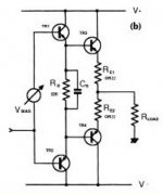
Add-on current dumping
Recently, several “non-switching” class-B amplifier circuits have been published. Some of these are complex, some have thermal runaway problems, and some require careful matching of devices.
This circuit is so simple that it can be implemented in any class-B amplifier, yet it is effective enough to cure all of the problems that traditionally result in crossover distortion.
The idea is to make sure that the output device is always turned on, by configuring it as a constant-current source when it would be normally be turned off. The principle is not new, but the realisation is.
Transistor Tr2 is forced into constant-current mode by collector current of Tr4. This transistor senses the fall in Tr2 collector current as I2RC falls, so I4RB4 directly compensates IORE negative feedback through Tr2 being the regulating current-derived negative feedback prevents thermal runaway without the need for special thermal feedback.
Take care selecting base resistor values RB3,B4. Lower values of around 200Ω are preferred to prevent creation of an additional pole within the desired bandwidth.
Drive current ID needs to be set at about twice the value of Tr3/Tr4 maximum collector current to allow the drivers to work in class-A throughout the full-voltage swing. Quiescent current is set by I3 and RB/RE.
Making RC equal to RE simplifies calculations.
Generating bias voltage with diodes allows a simple output current limiter to be added in the form of D3,D4.
Erik Margan
Ljubljana
Yugoslavia
Hi there,
for all interested, I have carefully retyped the original text of Margan's circuit idea. The scan of Albin's reprint thereof was very welcome, but I could see why Albin called it tatty. Anyway, I hopped into the technical university library last week to reclaim from history a couple of words that apparently had fallen of....
Enjoy your favourite records, without switching
Mark
Attachments
Last edited:
here we go again.
Ensuring that devices pass a minimum current, rather than turn off, does not make a ClassA stage.
Imagine the circuit as two single ended stages with that extra transistor added (to each half) to ensure the main pass devices always conduct.
What happens to the output when the deviation of the output current exceeds the bias current? It clips!
Last edited:
here we go again.
Ensuring that devices pass a minimum current, rather than turn off, does not make a ClassA stage.
Imagine the circuit as two single ended stages with that extra transistor added (to each half) to ensure the main pass devices always conduct.
What happens to the output when the deviation of the output current exceeds the bias current? It clips!
Hi Andrew,
ehhh, I dunno? By strict definition, I would be tempted to allow a "class A" badge. But I agree, heat- and trickery-wise, 'non-switching B' is not A.
I am afraid I don't grasp the reasoning behind the second part of your post. Clipping,,, WHY? The measurements published in Margan's article "Crossover distortion in class-B amplifiers" show not even a faint hint of clipping in NSB operation at levels exceeding bias.
regards and enjoy your albums!
Mark
Are there any news?
I would like to know commercial amplifier devices, where non switching ClassB is in use - except class XD from Cambridge Audio, go to
Amplifier Class-XD™
I would like to know commercial amplifier devices, where non switching ClassB is in use - except class XD from Cambridge Audio, go to
Amplifier Class-XD™
Hi
class-xd just shift the crossover distortion to a higher signal level, likely at a loudness too high to hear correctly considering that your aural compression is invoked at very low SPL.
Also, I think the limited definitions of class that applied to tube circuits cannot be imposed on solid-state. The latter has more flexibility so no devices turn off. However, since class is signal-referenced and one class-A def is that all outut devices contribute to the signal at all times, the NSW amps do not adhere to this definition. So - technically class-A that nothing turns off but not class-A with respect to signal. Therefore I agree with AndrewT
Last edited:
Its nice idea, easy to implement in Collector output stages as well in the non complementary N-Channel designs.
Hi there,
for all interested, I have carefully retyped the original text of Margan's circuit idea. The scan of Albin's reprint thereof was very welcome, but I could see why Albin called it tatty. Anyway, I hopped into the technical university library last week to reclaim from history a couple of words that apparently had fallen of....
Enjoy your favourite records, without switching
Mark
- Home
- Amplifiers
- Solid State
- margan : non switching class B