If all outputs are BJT, then Vbe multiplier works best for a standard double emitter follower output stage if it is mounted atop one of the devices.
This approach is recommended by Self, and I took his advice years ago and it's never caused a problem.
In my experience, once the amp has reached idle temperature and bias is accurately set (I use 0R47 emitter resistors to force more equal current sharing), after a busy session with lots of heat the bias generator slightly overcompensates, pulling back quiescent bias from 58mA to around 52mA, then slowly coming back up to 58mA after cooling re-establishes equilibrium.
The downside of this approach is the limited clamping pressure on the output because of the fragility of the TO126 package mounted on top, and the flying leads which must be manually attached to the Vbe multiplier and thence to the pcb. Clamping restrictions are ameliorated by using machined heatsink faces and appropiate thermal paste. However, as so often happens, and short of Bonsai's excellent smd solution, this is, to me, the optimal solution and I ain't goin' changin'........
Ciao,
Hugh
sakis, if you used ESP P03 as your test amp for where to put the sense transistor, I'm afraid you got it wrong. This amp has CFP type output and the thermal sensing must be done of the driver transistors never of the output transistors. There is an article on the ESP site explaining why.
Second that!
CFP is a completely different kettle of fish. It's biasing compensation is radically more sensitive.
I do not recommend the CFP output stage for Class AB because of the instability at the switching point, so I have not considered the biasing issues. Of course, this will draw critics, but it's only my opinion, and I'm sticking to it......
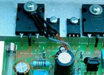
I have attached a picture of the Vbe multiplier mounted in one of my Lifeforce 55 amps.
I always prefer to use a TO126 rather than a TO92 because only the former has a metal base directly attached to the transistor die. This means that thermal conductivity to the sensing chip is FAR higher, and therefore bias tracking with temperature changes should be superior. Furthermore, unless a hole is drilled into the heatsink and the TO92 inserted with metallic glue, attachment is rather more difficult than use of a simple hole!
Hugh
CFP is a completely different kettle of fish. It's biasing compensation is radically more sensitive.
I do not recommend the CFP output stage for Class AB because of the instability at the switching point, so I have not considered the biasing issues. Of course, this will draw critics, but it's only my opinion, and I'm sticking to it......
I have attached a picture of the Vbe multiplier mounted in one of my Lifeforce 55 amps.
I always prefer to use a TO126 rather than a TO92 because only the former has a metal base directly attached to the transistor die. This means that thermal conductivity to the sensing chip is FAR higher, and therefore bias tracking with temperature changes should be superior. Furthermore, unless a hole is drilled into the heatsink and the TO92 inserted with metallic glue, attachment is rather more difficult than use of a simple hole!
Hugh
Attachments
Thanks Acid_K2
For bias compensation, I took the tack that I wanted the sensor to track one of the main power transistor die temperatures as quickly and closely as possible. This is the same approach used by On in the Themaltrak transistors where the diode and tansistor die are co-packaged. In my case, the SOT23 transistor has a very low thermal mass (so it responds to ambient temperature changes quickly). The idea of the thermal grease was to couple the collector lead which is the part of the leadframe on which the die sits in the transistor package to the whole sot23 device to ensure good coupling.
However, since the delta Vbe of th e sensing device is not the same as the output devices (I ignore the pre-drivers and drivers in this simplified explanation), you do not get exact tracking. If I had used a diode string to do the sensing, then one trick is to adjust the diode current and this allows some delta Vbe slope control. In my case, a little experimentation led to the conclusion that removing the thermal grease got the compensation just right. Without the thermal grease, the response is a little bit slower, but I have not measured it specifically - but I can detect it when I set the bias current up.
There is no one perfect way to do this - every set up has to be trimmed empirically because there are many variables brought about by the mechanical construction of the amp - size of heatsink, type of sensing, Output device delta Vbe charactersitics, etc. So, although I like 'my' approach because its very simple and mechanically easy to implement but this may well not be ideal for another type of mechanical design or layout.
")
For bias compensation, I took the tack that I wanted the sensor to track one of the main power transistor die temperatures as quickly and closely as possible. This is the same approach used by On in the Themaltrak transistors where the diode and tansistor die are co-packaged. In my case, the SOT23 transistor has a very low thermal mass (so it responds to ambient temperature changes quickly). The idea of the thermal grease was to couple the collector lead which is the part of the leadframe on which the die sits in the transistor package to the whole sot23 device to ensure good coupling.
However, since the delta Vbe of th e sensing device is not the same as the output devices (I ignore the pre-drivers and drivers in this simplified explanation), you do not get exact tracking. If I had used a diode string to do the sensing, then one trick is to adjust the diode current and this allows some delta Vbe slope control. In my case, a little experimentation led to the conclusion that removing the thermal grease got the compensation just right. Without the thermal grease, the response is a little bit slower, but I have not measured it specifically - but I can detect it when I set the bias current up.
There is no one perfect way to do this - every set up has to be trimmed empirically because there are many variables brought about by the mechanical construction of the amp - size of heatsink, type of sensing, Output device delta Vbe charactersitics, etc. So, although I like 'my' approach because its very simple and mechanically easy to implement but this may well not be ideal for another type of mechanical design or layout.
I just dug up this old post. My situation is a little different, I am doing 3EF but I use PNP as the pre-driver to drive NPN driver, which drive the NPN output transistor. I want to have the PNP pre-driver and the NPN driver thermally coupled together to cancel the temp coef of the two.
I cannot use the idea of Bansai as the pre-driver is going to have 50V across it rather a few Vbe across on the bias transistor. It is too much power dissipation using a SMD transistor as the pre-driver even if the current is only 10mA. ( 0.01A X 50V =0.5W).
So my option is to have the PNP screw on top of the NPN driver or put them on a separate heatsink where I can put the two transistor back to back, one on each side of the heatsink. ( both metal back of the transistors facing the heatsink surface, one on the other side of the heatsink.)
The lag time (response) of temperature change is much shorter with the transistor back to back on a separate heatsink as they are all metal to metal heat transfer. BUT there will be a temperature gradient between the transistor because the heatsink quickly spread the heat to the fins. So even the lag time is short, but the temperature does not track as well.
With the PNP mounting on top of the NPN ( plastic case), temperature tracking should be very good with no heatsink in between. BUT the lag time (response) is going to be much slower as heat has to travel through the plastic casing of the big transistor to the PNP.
question is anyone have real experience which one gives better result?
Thanks
there were cases in this forum that a pre-driver is followed by an opposite gender driver in a "folded" way, with a constant current source sourcing/sinking at the pre-drivers' emitter from/to the rails, and with the driver's output providing pre-drivers' collector supply on the opposite arm. Bob Cordell discussed it in his book, he calls it daimond-buffer-triple I think. I attempted it with On-semi ThermalTrack transistors at output with a very different thermal tracking scheme involving an opamp in this bench test case. It did indicate a good thermal cancellation between a pre-driver and a driver, as the bias voltage generator circuit only responds to the thermal sensors in the output transistors.
At least one other member, alan0354, documented his attempt of building this type of 3EF with conventional output BJT and a Vbe multiplier for bias tracking. I think he was successful in the thermal tracking part.
There could be other cases that I'm unaware of.
The pre-drivers in this diamond buffer triple see a very small Vce and power dissipation is very small too. However, TO-126 transistors are recommended in order for an easy mounting and to have a good thermal coupling with the driver transistors.
- Status
- This old topic is closed. If you want to reopen this topic, contact a moderator using the "Report Post" button.
- Home
- Amplifiers
- Solid State
- Can bias transistor mount on top(body) of output transistor??