Dear, Mr. Jan
I had bulid your LYNX 3 amp...
If I use 8 transistor output 5200/1943..with rail voltages +/-65 V 15 Amp traffo..at bias 300mv...
The sound are quite good and so powerfull..but I hear liltle hum at the ouput..no loud but its can be heard at night...
What should I do to remove the hum..? I isolated the main ground form the input with 10/1W R...but still ican hear the hum..
If I Put 8 Tr for the ouput..how many watts output for thats ?.. How I can measure for that..
Thanks...Dodi
Hi Dodi,
I have just read your email and this post here.
Lets take the main issue first: Hum
It would a be a big help, if you can make a drawing of the way you have connected the wires (Supply and Ground) to the PCB.
Hum can be caused by the Power Supply, the Ground wiring and by bad shielding..... Lots of possibillities......
Is your layout the same as the original, or have you made a different layout ?
Edit: Added photo of the original layout
Attachments
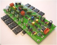
LYNX 3
Dear Mr. Jan.
Thanks to repply my email..
I had put away all the wires on the input..and only on min capasitor ground conected to ground via R10Ohm to chasis..
I conected the ground input on the PCB to power supply ground for the opamp and driver near them...because if I dont conenct them the DC Voltages are raise at the output stages...
According on your PCB layout, that ground input are not connected to anywhere..accept the feedback capasitor....
There's mistake on the layout..? I just download form the website in Grebers files...
Thank for your attention...
Dodi
 For curious reasons, I checked your Gerber files in Viewmate but the pads are minimal
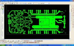
I opened a local file on my network disk, and had no problems with unit system...... 
Maybe I should try to check with the files on my website.
Perhaps they are corrupted in some way ........
Edit: Yes the files online are corrupted
Maybe the zip conversion did it??
I'll put up new files right away
Maybe I should try to check with the files on my website.
Perhaps they are corrupted in some way ........
Edit: Yes the files online are corrupted
Maybe the zip conversion did it??
I'll put up new files right away
It works now.... have you noticed my remark on Jens' pcb layout about the feedback? Your feedback point is a bit unsymmetrial, are you aware of that? You have also a couple of disturbing elements on the way to R120. A microscopic(?) improvement would be to "sniff" the feedback signal just before the inductor and have a clean trace directly to R120 with nothing else connected.
jan,
i'm using view mate but still unable to see the copper side correctly.
all tyhe lines are thin.
if you don;t mind,
can you post the pdf file for the board and its layout and
also can you provide a complete schematics?
some resistor don't have any value
there is not any voltage value
many thanks in advance.
dexter;
I have checked the Gerbers again, and see no problems......
Try doing a refresh on the site.
PDF-file can be found here:
http://www.audio-circuit.dk/PDF/LYNX_v3.0_Power_Amp.pdf
I have checked the Gerbers again, and see no problems......
Try doing a refresh on the site.
PDF-file can be found here:
http://www.audio-circuit.dk/PDF/LYNX_v3.0_Power_Amp.pdf
thanks han and peranders.
my mistake, the newer file is fine.
I can read them using guess
Jan,
What're the voltage that you use for the amplifier and driver?
Are you using regulated supply for the driver?
why you don;t put some caps bank near the o/p Tr?
did you make any single side pcb layout?
sorry for asking too much questions.
many thanks for your design.
best rgds,
- Status
- This old topic is closed. If you want to reopen this topic, contact a moderator using the "Report Post" button.
- Home
- Amplifiers
- Solid State
- Lynx 3