A few more modifications/optimizations - the topology has a name now, 'Moksha', which loosely translates (from Sanskrit) to Liberation; Salvation; Higher Consciousness; etc.
I broke through -120 dB in the THD20 simulation - H2 is now at ~-127 dB, H3 at -133 dB, H4 & H5 below -145 dB, everything else below -150 dB. The main change is a 2nd-order lag-lead compensation network consisting of R52, R55,C2 & C13, which greatly improved the harmonics. I also switched to more garden-variety BJTs wherever possible, without significant impact on the THD numbers. The O/P stage has also reverted back to a single c5200/a1943 pair. Iq in the output stage simulates at 0.2A, which is a bit higher than I'd like - I'll try to lower that later if the impact on the THD is acceptable.
After this point, further circuit elaboration will concentrate mainly on developing a practical, inexpensive, stable, reliable and easily-built real amplifier with commodity parts - the quest for improved THD goes on the back burner.
Attachments
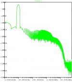
linuxguru said:And here's the FFT plot for 20 kHz, ~40V amplitude output into 8 ohms.
Looks very good.
How does it go into harder loads 4 / 2 ?
T
Thanks - it wasn't designed for 2/4 ohm loads; the SOA of the single O/P pair will definitely be exceeded at full voltage swings. However, Spice doesn't care about the SOA, so it will happily simulate and give phantom results for 2/4 loads - I'll run a sim later for these loads.
It should be possible to modify the design with an additional paralleled pair or more O/P transistors (which was how some of the intermediate designs looked), for 2/4 ohm loads.
It should be possible to modify the design with an additional paralleled pair or more O/P transistors (which was how some of the intermediate designs looked), for 2/4 ohm loads.
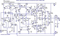
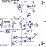
Another redesign/iteration of Moksha - the topology is broadly similar to the earlier ones, but there are major changes in a number of areas, all of which contribute in improving the THD20 numbers to ~-140 dB (H2 ~= H3) at ~50W into 8 ohms:
1) The LTP/Input stage and the VAS have been flipped over in polarity from the previous iteration - this allows NPNs to be used in many high-gain locations, and relegates the PNPs to gain-insensitive locations like the LTP, Wilson Current Mirror and Vbe Servo.
2) The active load circuit for the LTP has been modified from the earlier design, which was itself modified/derived from an earlier idea of Bob Cordell's posted here at DIYaudio. The new design separates the base drives to each of the active loads, and gives better stability as well as a few dB improvement in THD numbers.
3) The Kulish cells are retained, with minor changes to the resistor ratios, which are not critical.
4) The pre-driver stage is entirely new and novel - it uses two baxendall super pairs in conjunction with a floating current mirror to drive the driver/output stage. I have not encountered this topology in the literature, but it is deceptively simple and gives outstanding results.
5) The rails have been lowered to +/- 35V to allow operation well within the SOA of a single pair of 2sa1943/2sc5200. The maximum designed output power is now about 55W into 8 ohms.
6) All the small-signal transistors are jelly-bean, commodity types; except for the output devices and drivers, all components shown are commodity types priced at a few cents each.
A few other minor refinements/elaborations are incorporated. The schematic follows:
Attachments
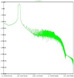
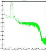
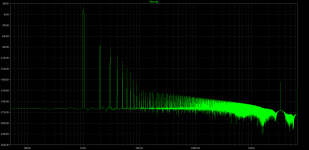
FFT plot for Moksha-50W
Here's the FFT plot for a 20 kHz, ~30V amplitude signal at the output, corresponding to ~50W into 8 ohms. H2 ~= H3 = -140 dB; almost all higher harmonics are <-150 dB.
The output stage is biased to Class-AB at the edge of Class-B; bias current is not critical and can range from 50 mA .. 300 mA or higher.
Attachments

> Should sound very, very clean without being surgical.....
Hugh - thanks, I'm certainly planning to build it eventually, hopefully after improving its stability. You'll notice that I've tried to incorporate some of your design principles in it - notably:
1) wideband circuit structures that allow relatively easy substitution of commodity devices at most locations;
2) relatively slower and linear devices in the LTP and VAS wherever possible;
3) avoidance of active current source(s) and current mirror(s) in the LTP;
4) fine-tuning of sonics achieved mainly through the compensation schema;
5) avoidance of asymmetric base-collector lag compensation (there is however a symmetric RC lag element in the VAS which is not that toxic to the sonics);
6) your preferred choice of Toshiba drivers and output devices (they simply happen to be the best deals going at the moment, and I have good Spice models for all four of them: a1837, c4793, a1943 & c5200).
I'm presently still fiddling with the AKSA 55W work-alike - whose sonics appear to be quite sensitive to the bypass, bootstrap and input capacitors, not to forget the compensation schema. Hopefully, the capacitor dependencies will be somewhat reduced in Moksha to just the input caps and the main rail filter caps.
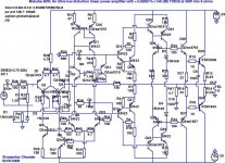
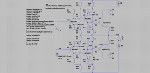
Input/VAS stage modifications
Here are some further modifications to the topology of the LTP and VAS stages, with the everything else removed for the purpose of LTSpice simulation. The main change is the use of Lender's dual drive to both the LTP active loads. All transistors are garden-variety commodity types.
It simulates with H2 ~= -126 dB, H3 < -145 dB, ... at VAS voltage swings of +/- 40 volts. Most importantly, even harmonics dominate the succeeding odd harmonics by ~20 dB each, potentially yielding tube-type sonics, but with vanishingly low THD.
Attachments
Member
Joined 2009
Paid Member
Hi Linuxguru
did you asked the moderators to allow pornography
http://www.diyaudio.com/forums/atta...or-class-ef-o-p-stage-discrete_opamp1_fft.jpg without the balls?
did you asked the moderators to allow pornography
http://www.diyaudio.com/forums/atta...or-class-ef-o-p-stage-discrete_opamp1_fft.jpg without the balls?
Member
Joined 2009
Paid Member
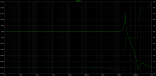
Is that -105dB for 2nd & 3rd, for an output stage without global NFB?
What is that @ ~ 23MHz?
unfortunately it is global cfb.
~ 23MHz is the oscillation
tomorrow I will send asc file to play with
- Status
- This old topic is closed. If you want to reopen this topic, contact a moderator using the "Report Post" button.
- Home
- Amplifiers
- Solid State
- Kulish Corrector for Class-A EF O/P Stage