Planning to make a new layout of the NAP140 and NCC200.Who can provide me the latest schematic and suggestions regarding the best output and pre driver trannies etc.
Hi meanman1964,
Here's my interpretation of a NAP140/NAP140 Clone/NCC200. Untested, and transistors may not be optimal.
If you PM me your email address I can email you all the documentation I have collected from the web.
regards
Attachments
BC550/560 are only 50V Vceo small signal transistors. As the schematic specifies, you can use these at the input, TR1/2. Originals elsewhere are 80V MPSA 06/56 or similar BC546/56 can be used. These suit the general voltage levels. However, you can't just use the cheapest available parts if you want good sound and for the amplifier to work without failure. TR4/5 must be fast, higher voltage and Ft types for the VAS. If you can't buy any type covered in this thread (many different types are supplied in kits) then you could use the old BD139/40 for VAS or drivers but there is always a compromise with such part swapping.
IMHO, many parts will work as you suggest, if you pay attention to the transistor specifications but "to work" and "to be best suited" are not the same.
IMHO, many parts will work as you suggest, if you pay attention to the transistor specifications but "to work" and "to be best suited" are not the same.
DC offset in Naim 140 C
Hello everyone. I am having trouble getting DC offset on one board down to the same level as the other one. The good one is measuring 30mv with no speaker that seems acceptable to me. The other one measures 300mv which is way too much. I tried all measurements possible, both boards have the same parts and measure the same at all critical checkpoints except at the input LTP. At the bases of the two transistors I measure 350mv and 360mv in one board and 25mv e 35mv in the other (the good one!). All transistors checked and resistirs checked and rechecked. The same ~300mv higher reading shows of course the collector of Q3 (tail) and then flows through to the output. Any clues where I should look at? Could just be poor LTP transistors matching? I am using B550 for LTP and Q5, ZTX for VAS, MJ15032/3 drivers, MJL3281 output biased at 30ma. Current across R 15 and R 18 is 9.75ma and 10.75ma in both boards (I thought they should measure the same, is this close enough?)
Thanks a lot for any help, it is driving me crazy
Thanks Ian. I've read up more after I've posted. Found the Avondale NCC schematic and I'll build the amp based on it. BC546 for TR1/2/3, ZTX753 for TR4, 2N5551 for TR5 and ZTX653 for TR6.
This project was supposed to be a quick and easy build with available parts on hand but as always after reading and research I'll be making it a dual mono with the right parts.
This project was supposed to be a quick and easy build with available parts on hand but as always after reading and research I'll be making it a dual mono with the right parts.
BC550/560 are only 50V Vceo small signal transistors. As the schematic specifies, you can use these at the input, TR1/2. Originals elsewhere are 80V MPSA 06/56 or similar BC546/56 can be used. These suit the general voltage levels. However, you can't just use the cheapest available parts if you want good sound and for the amplifier to work without failure. TR4/5 must be fast, higher voltage and Ft types for the VAS. If you can't buy any type covered in this thread (many different types are supplied in kits) then you could use the old BD139/40 for VAS or drivers but there is always a compromise with such part swapping.
IMHO, many parts will work as you suggest, if you pay attention to the transistor specifications but "to work" and "to be best suited" are not the same.
At the bases of the two transistors I measure 350mv and 360mv in one board and 25mv e 35mv in the other (the good one!). All transistors checked and resistirs checked and rechecked. The same ~300mv higher reading shows of course the collector of Q3 (tail) and then flows through to the output.
Hi,
If the base voltages at the LTP are similar then the feedback is working as supposed to. Assuming that the resistor values are OK I would troubleshoot in this order (following the eBay circuit):
1. Make sure that input capacitor C1 is OK and not a leaky one.
2. Do the same for feedback capacitor C5.
If fault is still there:
3. Check the voltage across the current source resistor R21. The working channel is big advantage, because you can compare. Current of 0.8-1.2 mA through R21 is OK and should be similar for both channels. If it's not,
check LTP transistors base to emitter. You should see ~0.5-0.6Vdc. If close to 0V or higher than, say 0.75V, transistor is faulty.
If OK:
4. Do same check for the current source transistor.
If current source is fine as well, then I would say the problem is something silly like solder drop shorting somewhere, or cold solder joint, or ground not attached to the right place, or input connected on the wrong side of the input capacitor etc. in this line of thoughts...
Ruwe, thank you for our precious input as always. I checked everything that you mentioned, current source is okay, all transistors drop 0.6v, capacitors orientation is okay, no continuity between capacitors ends, the boards are a bit beat up because of experimentation but could not find obvious faults. Current source is constant at ~1.2ma and approximately equal to the sum of the measured through the 2 top resistors in the LTP. The ~300mv appear at the base of both LTP trannies. Q5 emitter measures 1.4V, collector ~0.4v, it seems reasonable. I have no protection circuit. Need to let it cool and think it through. Anything else you can think of?
Troubleshooting is frustrating but very informative
Troubleshooting is frustrating but very informative
Anything else you can think of?
Hi,
LTPs following each other is OK, they are supposed to do so. The question is which base is leading the change from 0mV to 300mV (the other base is just following). At first I thought it should be the input (e.g. leaky cap), but you say it is OK. LTP transistors sharing current equally means they're OK as well. The feedback cap is also not leaky, right? ... By the way, caps may be leaky and still measure as high enough resistance. If you're out of useful ideas, why don't you swap them with the other board and see whether the fault moves with them.
Something very important: make sure that the input ground is connected to the feedback ground, i.e. the feedback capacitor. They should be on the same path on board.
In this circuit ground is the reference point, if ground is not the same on both sides of the LTP the circuit will balance itself somewhere where it finds it most comfortable, between two different "references". Also make sure that the output ground (Zobel and speaker out) is connected together with the input ground to the power supply common. I remember the eBay circuit had two separate grounds (input and output) and they should be linked or both must be soldered to the power supply common. I'm sure you know that, but check that's valid for this particular channel. Sometimes when all wires are spaghetti like, one can omit something ... Check that nothing is touching the case, if not supposed to ... like speaker terminals or input jacks with missing plastic insulators ... stuff like that.
Did you try this channel with music? Is it working at all? You can try it with some cheap speaker connected through a big cap (like in a single-ended amp), thus isolating the DC component during the listening test. It's important to know whether the amp works without distortion.
If it's playing music nicely, the only thing left to unbalance the DC offset are the resistors, you know the rule: R2+R3=R8+R9 (ref. eBay schematic).
Troubleshooting can be frustrating
First rule is "check the obvious and the easiest".In general, circuits with feedback loops are the most difficult to troubleshoot, because it's never clear what's causing the fault, everything is affected through the feedback, sort of "the chicken or the egg" dilemma. Luckily, in this circuit, there is only one feedback loop!
If you're out of reasonable ideas, try something practical. Swapping suspicious parts is big helping tool, comparing with working circuit is another one.
Last edited:
hi all
ım try to complate my nap140,ı complated my pcb and heatsink,at the last making psu is rest.
now ım wondering that is nap140 class b or ab? its biased to 40 ma if no signal at input.
40ma is enough for the class ab, if not how much bias is needed for class ab?
thanx inadvance to one who will replay.
hi all
now ım wondering that is nap140 class b or ab?
Hi,
I'd say it's closer to class B than AB, but it doesn't matter much anyway. According to Douglas Self's book properly executed class B outperforms class AB, because "gm doubling" is avoided.
ı think tommorrow ı make a testing so to how much mA should ı biase the amp to work as class ab and b,
ı wanna hear classes differances ıf ı can,or ı want to see advantages or disadvantages classes differences.
My supplay volatges is 35v dc,and output transistors 2sc5200.
ı wanna hear classes differances ıf ı can,or ı want to see advantages or disadvantages classes differences.
My supplay volatges is 35v dc,and output transistors 2sc5200.
NAP140
I complete my nap140 today,
and did some test,its imprresd me,mid and treble so good bass frequency is enough for me.
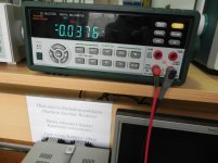
I set it 50ma when no signal input,but after giving 80mv 1khz the current taken from psu be 240ma,it that sutiation amp not so hot its resanable temperature.It increases to 450-500ma when 1v apears in the input,and getting much more hot like class a.
Maybe setting to 75ma bias when no signal on the input make thesound little warmer.I'll try it
I like the amps sound,tomorrow ı will do a couple of test and after pakaged it to its case
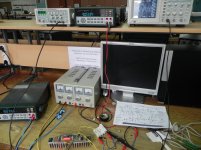
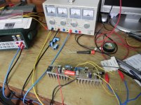
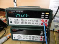
some measuerment are on the photos.
1.photo is general sight
2.is +/-30v psu
3.is output offset voltage
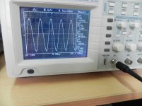
4.is view of the output signal on the 9ohm resistor connected to amps output
5.is bias current
I complete my nap140 today,
and did some test,its imprresd me,mid and treble so good bass frequency is enough for me.
I set it 50ma when no signal input,but after giving 80mv 1khz the current taken from psu be 240ma,it that sutiation amp not so hot its resanable temperature.It increases to 450-500ma when 1v apears in the input,and getting much more hot like class a.
Maybe setting to 75ma bias when no signal on the input make thesound little warmer.I'll try it
I like the amps sound,tomorrow ı will do a couple of test and after pakaged it to its case
some measuerment are on the photos.
1.photo is general sight
2.is +/-30v psu
3.is output offset voltage
4.is view of the output signal on the 9ohm resistor connected to amps output
5.is bias current
Attachments
Last edited:


Got it thanks! I am aware of the separate grounding etc.,...will double check. A couple of components question: 1) the R2+R3 = R8+R9 combo. The former is a low pass filter that varies from 100khz with 4k7 resistor to more than 260khz with 2k7 or 3k. Is there one combination which is preferable to the other? (ie 22k + 4k7 vs 22k+4k7 or 25k+3k). Also the total resistance of R8+R9 = 28K should it be matched perfectly (none of the circuits do, it is mostly 26.7K)
2) I have 10 ohm resistors available instead of 8.2 ohm for the output to ground, what is the impact of changing this?
3) pre-drivers: ztx or toshiba 2sc2705/a1145?
Apologies for the abuse!
2) I have 10 ohm resistors available instead of 8.2 ohm for the output to ground, what is the impact of changing this?
3) pre-drivers: ztx or toshiba 2sc2705/a1145?
Apologies for the abuse!
Which is the best way to protect NAP140 clone from thermal runaway?
I was wondering which is the best way to "protect" a NAP140/ncc200 clone against excessive current draw such as happens with thermal runaway and perhaps oscillation.
Recently I had a mishap with a pair of Naim/ncc200 clone boards which I had bought a long time ago and had given up on previously because they didn't sound great.
I replaced all of the chinese parts with quality alternatives and used some spare Toshiba sc5200s driven by mje13034/mje13035.
All measured well with bias current at 36ma through the +ive rail and dc offset less than 10mv at the speaker terminals. They sounded good too.
After I'd finished listening to the music, I left them on while I did other things.
About half an hour later when I came back I found that the driver on the +ive side of one board, the one on the -ive side of the other had been heated to a high temperature and had burnt the board and adjacent components very badly and also badly burnt the track to the base of each output transistor. It really looked awful. Happily both speakers survived (thanks to Rod Elliott's speaker protection module).
I'm still wondering why this happened because it measured well and seemed to be thermally stable. Were the drivers not compatible with the sc5200s? The Sc5200's were very well heatsinked and the drivers had heatsinks as well.
But my main concern is what is the best way to safeguard against such an event apart from actually preventing it.
I had a 3amp slow blow fuse in the mains input but that really only protects against a short circuit.
A 2 or 3 amp fuse in each of the amplifier voltage rails (+/-43v) would work I think. But what would happen if (say) only the fuse on the +ive rail blew? From what I understand, disconnecting one of the rails while leaving the other intact is likely to cause great damage to the amplifier and speakers.
So what is the best way to protect against these sorts of events?
1) the R2+R3 = R8+R9 combo. The former is a low pass filter that varies from 100khz with 4k7 resistor to more than 260khz with 2k7 or 3k. Is there one combination which is preferable to the other? (ie 22k + 4k7 vs 22k+4k7 or 25k+3k). Also the total resistance of R8+R9 = 28K should it be matched perfectly (none of the circuits do, it is mostly 26.7K)
The low pass filter frequency depends not only on R3, but also on your source impedance. You have to look at the input from the base of Q1 back to the source similar to the way it's done using Thevenin theorem.
For example if your source impedance is 1k it will add to the R3 when you do the calculations. If you're using passive preamp then the filter frequency will change with the rotation of the potentiometer, with highest resistance when the potentiometer is set to 50/50, and lower in both ends. And, of course, you have to add R3 to that in the final calculation. So, as you see, the optimum value of R3 is flexible in accordance with the source impedance and the chosen input freq. bandwidth. I'm using 1.5k + two resistors of 56k in parallel for R2.
As for the R8, R9 matching with R2, R3 - it is not critical, especially if you use high gain LTP, because the base currents will be almost non-existant, so will be the "error" voltage drop across the resistors. Actually, if we take only the DC condition the equation should be R2+R3=R9 (in DC, R8 is blocked by the capacitor C5). You can play with the resistor values if you want to shape the offset close to perfection, but if the transistors have reasonably high gain of >250 the offset will be close to 0mV even with slightly mismatched resistors. The other factor affecting the offset is the base-to-emitter matching of each of the LTP transistors.
That's why I think that in your faulty channel you have heavy resistor mismatch or base biasing problem (high "error" current) in one of the LTP transistors ...
I don't think it's very important. This is part low-pass filter, part buffer for the EMF coming back from the speaker coils. IMO, not very critical and ideally should be experimentally determined as a function of the amp HF stability, speaker cables and speakers used. Anything between 4 and 10 ohms is OK in combination with 100nF. 220nF in this circuit is slightly more than the standard.2) I have 10 ohm resistors available instead of 8.2 ohm for the output to ground, what is the impact of changing this?
I have no idea. Pick something with wider bandwidth and power capability of several watts. Not fake ones are always preferable3)re-drivers: ztx or toshiba 2sc2705/a1145?
Well, I broke my rule of not discussing electronic theory in threads
I hope it will help you in troubleshooting, though.- Home
- Amplifiers
- Solid State
- NAP-140 Clone Amp Kit on eBay