By the way, I would like to buy the pair of PCB also. It will speed up development dramaticley. And, to be honest, your warning about how PCB layout is critical stops me from redesigning it. If you, Roender, will place order for PCB manufactoring, pls, remember me as well.
And, pls, excuse my english (for all).
And, pls, excuse my english (for all).
Dear fellows,
Thank you all for your interest in building my amplifier.
Regading PCB request, I've left with two RMI-FC100 PCB peers unused. The price is not small, 45EUR for one stereo amplifier, because all of them was made as a prototype in a very small quantities.
If I have to make 50 peers, the PCB shop price will be only 22Eur for two RMI-FC100 boards (one stereo amp).
I don't know if it's rentable for you to buy at this "prototype price" because you must add shipment cost. Maybe in an envelope will be much cheaper ...
If you can organize a group buy, I will put an order for 50 peers of two. It will take 7 working days for shop to make the boards and I will send all of them to the GB organizer.
The PCB for regulated front end PSU was made "in house" with the help of an press and peel blue paper. This one was much simple to make because it has only one layer.
On the other hand, maybe you can get a better price from a local PCB shop and you can use gerber/exelon files attached earlier in this thread.
Mihai
DRZ1 said:
Shure, i am already on it ( pieces supply).
It's possible the pcb must be modified to fit my case. Roender do you have somethink you want to try? I have acces to a milling prototype machine for the PCB, it's more easy than etching it.
Hi DRZ1,
I don't know what is this "milling prototype machine" and what type of files can be use to make boards.
I can send to you all CAD files if you want to make some changes but I must warn you that you will need a valid EAGLE license because the PCB dimensions is over maximum permissible free version size.
Mihai
spind said:
I'd like to.....but I'd need some guidance ...
... What is the width of the boards plus output transistors (to check if my my heatsinks are OK). What are the transformer requirements; how much latitude is there with the supply voltages?
thanks,
Steve.
Hello Spind,
You will have my support!
The amplifier PCB dimmensions are:
205 x 63 mm for PCB only
205 x 97 mm for PCB and Power BJTs
For power stage only you will need one 400...500VA 4x25V or two 200...250VA 2x25V transformers. For the front end PSU you will need one 30VA 4x34V or two 15VA 2x34V transformer.
WARNING FOR THOSE WISHING TO DESIGN THEIR OWN PCB
An amplifier of this complexity requires careful layout. Stability is a primary concern in any feedback amplifier. My commercial amplifiers often require extensive pcb design work, and some have taken more than 100 hours at the PC to yield an elegant, functional and easily constructed module.
Good layout is not trivial, it is an art, and many electrical parameters and layout issues must be considered. This all takes time and often considerable iteration. This is expensive.
I strongly suggest interested parties support Roender's layout with a group buy; it clearly works very well and looks very slick.
Cheers,
Hugh
lumanauw said:Hi, Roender,
There's a patent of distortion reduction for topology using folded cascode+current mirror.
Patent #5166637
I'm working on it, see http://www.diyaudio.com/forums/showthread.php?postid=1349231#post1349231
lumanauw said:Hi, Roender,
There's a patent of distortion reduction for topology using folded cascode+current mirror.
Patent #5166637
Thank you David.
Patent #5166637 is an earlier blueprint of Scott Wurcer's AD797. Who will need such complexity for an power amplifier?
That clever current error correction around folded cascode VAS and output stage is unnecessary for an class A output stage.
Mihai
aparatusonitus said:
Hi apparatus,
why not make an own thread? I like your approach.
Rüdiger
Hi, Roender, aparatusonitus,
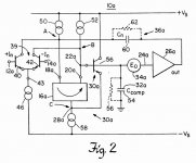
I never built/use this correction system, so I don't know much about it, but looking at your schematics, it is quite easy to experiment with it.
If you look at this attachment, the correction system is possible because there is a "virtual" inverting input of the output stage, that is point A.
The correction works optimal if impedance of "32a" (that is element 56+54) is the same (calculate the gain first) to the impedance of "36a" (that is element 62+60).
In your schematic, element "32a" is C8//C9.
(In aparatusonitus' is C12//R38)
You can try this correction system by putting C from output node (before L) to emitor of Q14. Initial approximation value could be 30pf (C8//C9), but it must be adjusted in the real amp.
(in aparatusonitus' amp, put another 47p//165k from output to emitor of Q11a)
Attachments
roender said:
Hi DRZ1,
I don't know what is this "milling prototype machine" and what type of files can be use to make boards.
I can send to you all CAD files if you want to make some changes but I must warn you that you will need a valid EAGLE license because the PCB dimensions is over maximum permissible free version size.
Mihai
It's a milling machine specialised for milling PCB board. It's used for testing PCB design before production. Works with gerber files. I use Protel soft.
http://www.mitspcb.com/
Denis
lumanauw said:
You can try this correction system by putting C from output node (before L) to emitor of Q14. Initial approximation value could be 30pf (C8//C9), but it must be adjusted in the real amp.
(in aparatusonitus' amp, put another 47p//165k from output to emitor of Q11a)
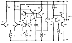
Hi lumanauw,
A and B nodes are input and output nodes of current mirror, so in my sch C3//R34 have to be connected to collector of Q11A, not emiter, see sch below.
Attachments
lumanauw said:Hi, Roender, aparatusonitus,
... looking at your schematics, it is quite easy to experiment with it.
If you look at this attachment, the correction system is possible because there is a "virtual" inverting input of the output stage, that is point A.
The correction works optimal if impedance of "32a" (that is element 56+54) is the same (calculate the gain first) to the impedance of "36a" (that is element 62+60).
In your schematic, element "32a" is C8//C9.
(In aparatusonitus' is C12//R38)
You can try this correction system by putting C from output node (before L) to emitor of Q14. Initial approximation value could be 30pf (C8//C9), but it must be adjusted in the real amp.
David,
The distortion cancelation method, a la Wurcer's ad797, is applicable only if you have the same impedance, as high as possible, into the input and the output of the current mirror. In my design there is no floating current mirror and the input has low impedance compared with the output.
I am not sure if it is possible to implement AD797 topology in a discrete power amplifier.
Mihai
roender said:I am not sure if it is possible to implement AD797 topology in a discrete power amplifier.Mihai
Hi Mihai,
Before I went this road in design, I have ask the man himself, Scott Wurcer, whether is it possible to design AD797 style discrete preamp/opamp…guess you know the answer.
aparatusonitus said:
Hi Mihai,
Before I went this road in design, I have ask the man himself, Scott Wurcer, whether is it possible to design AD797 style discrete preamp/opamp…guess you know the answer.
It is pointless ... because for a discrete preamplifier you can use an class A output stage, well ... it is highly recommendable to do that!
The cancelation method described in US patent 5166637 is applicable only if you want to avoid high power dissipation in output stage.
roender said:
The cancelation method described in US patent 5166637 is applicable only if you want to avoid high power dissipation in output stage.
I have tried to sim my sch with and without cancellation network, and IIRC got something like 25dB less H2 with cancellation network (not that I’m a THD freak). Try to look at it as a first experiment if I ever decide to build a power amp upon it.
forr said:
I think you use Baxandall's constant current sources.
No high frequencies problem with them ?
I have not notice any HF problems in sim (mind you I’m not an EE and will never be, I have just keep notes from the gurus here
 ), but as usual I have to build the real thing first to see wether it oscilates or not.
forr said:
What's the purpose of the CCS around Q5 and Q6 ?
Wrong copy/paste move, just neglect all schebang around them.
- Home
- Amplifiers
- Solid State
- RMI-FC100, a single stage audio power amplifier