I'm sorry for the esoteric question here, but I asked Analog Devices directly and they have yet to respond. My two questions are about the Alexander Power Amplifier from an Analog Devices Application Note:
AN211
http://www.analog.com/UploadedFiles...211.pdf&fterm=alexander&fterm=alexander&la=en
Just to give a brief heads-up, it is a current feedback-type power amplifier that also uses the power supply pins of opamps to carry the signal in the input section of the circuit.
1) I understand why A2 was added to the circuit (to reduce the DC offset at the output of the power amp). Even though A2 is specified to be a very low offset opamp, how can we be sure that it will contribute a low offset when we are using its power supply pins as outputs (instead of its conventional output pin)? How can we be sure that if we use the output pins themselves of a low offset opamp, they will contribute to a "low offset" of the overall audio amp at its output?
2) The author stated that the two compensation caps (C6 and C7) were originally placed from their respective nodes to ground - then they were later removed from ground and tied together at the output of opamp A1. Did the author have insight and prior know-how to do this, or was it a mere guess and check approach that happened to provide better results?
One of the most famous here:
http://www.diyaudio.com/forums/showthread.php?threadid=36563&highlight=
http://www.diyaudio.com/forums/showthread.php?threadid=36563&highlight=
if the op amp is low offset from output to ground, it's reciprocal is also true, that the differential from output to power supply pins is also "low offset". op amps get their "ground" reference at half the difference between supply rails, so what "low offset" actually means is that the output pin is very close to the midpoint between the supply rails. the op amp still behaves in the same manner internally, but it's externally measured behavior is opposite, since it's the reference that's being changed rather than the "signal". in a way it's very similar to the functioning of a QSC amp, where the speaker output is taken from the midpoint of the power supply, and the amp output "drives" ground (actually it floats the power supply rails using ground as a "leverage" point).
Opamps don't care about ground, and they don't get their ground reference from half the supply voltage. Have you noticed that opmaps don't have ground pins?
Opamps care about the differential voltage between input pins. The offset of an opamp is determined almost entirely by the input stage, all other sources of offset are within the feedback loop and as such are negligible.
Opamps care about the differential voltage between input pins. The offset of an opamp is determined almost entirely by the input stage, all other sources of offset are within the feedback loop and as such are negligible.
They don't though.
The output stage has no natural output voltage, no voltage towards which it tends. Within its operating limits, an opamp's output voltage is defined by its input, the opamp doesn't care if one of those inputs is labeled ground by the designer.
Think about PSSR.
Once again, offset voltage is overwhelmingly a function of the input stage. Edit: Even when the output is taken from the supply current.
URL is death. use this URL:I'm sorry for the esoteric question here, but I asked Analog Devices directly and they have yet to respond. My two questions are about the Alexander Power Amplifier from an Analog Devices Application Note:
AN211
http://www.analog.com/UploadedFiles...211.pdf&fterm=alexander&fterm=alexander&la=en
Just to give a brief heads-up, it is a current feedback-type power amplifier that also uses the power supply pins of opamps to carry the signal in the input section of the circuit.
1) I understand why A2 was added to the circuit (to reduce the DC offset at the output of the power amp). Even though A2 is specified to be a very low offset opamp, how can we be sure that it will contribute a low offset when we are using its power supply pins as outputs (instead of its conventional output pin)? How can we be sure that if we use the output pins themselves of a low offset opamp, they will contribute to a "low offset" of the overall audio amp at its output?
2) The author stated that the two compensation caps (C6 and C7) were originally placed from their respective nodes to ground - then they were later removed from ground and tied together at the output of opamp A1. Did the author have insight and prior know-how to do this, or was it a mere guess and check approach that happened to provide better results?
https://www.analog.com/media/en/tec...tes/58052492001115525484056221917334AN211.pdf
URL is death. use this URL:
https://www.analog.com/media/en/tec...tes/58052492001115525484056221917334AN211.pdf
Thanks for doing forum library work! Btw, I've seen it few times, it's funny, the link is not "death", it's dead.
")
you are right, but the activate spell checker accept both spellings.
I am looking for commercial amplifier models used this mentioned topology under
https://www.analog.com/media/en/tec...tes/58052492001115525484056221917334AN211.pdf
and tested here:
Home Page | Stereophile.com
thank you for an advice.
I am looking for commercial amplifier models used this mentioned topology under
https://www.analog.com/media/en/tec...tes/58052492001115525484056221917334AN211.pdf
and tested here:
Home Page | Stereophile.com
thank you for an advice.
Last edited:
yes - thanks for that advice; go to attachment and the stereophile review under
Arcam DiVA A85 integrated amplifier Measurements | Stereophile.com.
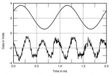
Distortion waveform (fundamental notched out) don't looks good, because high order distortion components are superimposed on ear-friendly third harmonic wave form. I guess the sound is harsh and crispy.
Maybe the P85 (power amp version) looks better, because there are no MCU operating board/RC receiver/X-TAL in use and thus no unwanted (aliasing) effects by RF interference transmission in the audible spectrum.
Are there in the meantime such power amplifiers with modern operational amplifiers like OPA1611/OPA1612 ?
Arcam DiVA A85 integrated amplifier Measurements | Stereophile.com.
Distortion waveform (fundamental notched out) don't looks good, because high order distortion components are superimposed on ear-friendly third harmonic wave form. I guess the sound is harsh and crispy.
Maybe the P85 (power amp version) looks better, because there are no MCU operating board/RC receiver/X-TAL in use and thus no unwanted (aliasing) effects by RF interference transmission in the audible spectrum.
Are there in the meantime such power amplifiers with modern operational amplifiers like OPA1611/OPA1612 ?
Attachments
Arcam used the topology in some of their amplifiers, the DiVA A85 is one i think
Yes, but I suspect Arcam changed the compensation scheme because the main feedback loop is only conditionally stable with Alexander's arrangement. The topology as a whole is of mediocre linearity.
Last edited:
Yes, but I suspect Arcam changed the compensation scheme because the main feedback loop is only conditionally stable with Alexander's arrangement. The topology as a whole is of mediocre linearity.
Old thread, but yeah.. also Alexander's original was using IGBTs. I have also seen it built using MOSFETs. Arcam also changed the current mirror scheme for Wilson mirrors.
Arcam also changed the current mirror scheme for Wilson mirrors.
Actually, Alexander's scheme also uses Wilson mirrors; however, he uses diodes where BJT transdiodes would ordinarily be employed, and this is unfortunate because, according to Baxandall, a transdiode gives better matching than an ordinary diode.
Last edited:
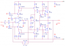
here is an other circuit, but only slightly different
https://web.archive.org/web/20100114165248/https://www.angelfire.com/sd/paulkemble/sound8.html
https://web.archive.org/web/20200220201123/https://www.angelfire.com/sd/paulkemble/sound8.html
because the URL is dead I have save the schematic and circuit description here:
Alexander fast FET
This design is very close to that by Mark Alexander ('The Alexander Current-Feedback Audio Power Amplifier', Analog Devices Application Note AN-211, Audio Products 4-57/71) which contains much detail including PCB, component and wiring layouts whilst quoting a lower slew-rate, >200V/µS. If the reader is considering constructing this amplifier, perusal and study of the application note is recommended.
(Precision Monolithics Inc SSM-2131 datasheet, 6/89, rev A, p7).
With V+/V++ and V-/V-- ±40V and quiescent set at 300mA,
THD (50W into 8 ohms) = 0.002% @ 1kHz and 0.007% @ 20kHz.
IMD = 0.0017% (50W into 8 ohms).
Flat to 1MHz (-3dB).
Slew rate = 300V/µS.
Gain = 24.
DC output offset = 1mV.
No RC compensation to ground or output inductor required.
All unspecified Rs 1%, MF, ¼W.
Input buffer gain can be increased from 1.5 to 10 before bandwidth drops (33R2 resistor set to 1R8, or 16R5 to 299). Capacitive load compensation can be given, if needed, with components marked 'TBD'. Operation to ±100V feasible with additional output pairs, for outputs of several hundred watts.
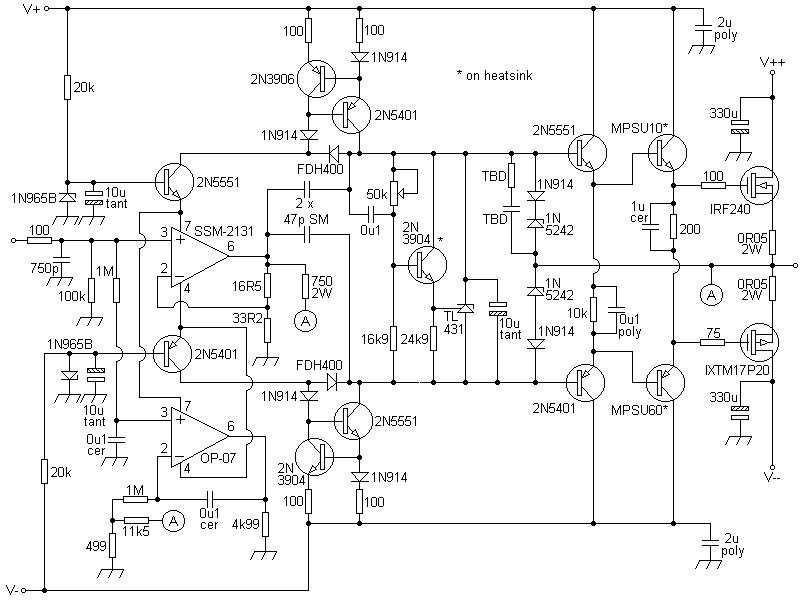
The driver load of 1µF paralleled with 200R can, given output layout, be conveniently built up using paralleled components, eg; 10 x 0µ1F //'d with 5 x 1k.
A very compact build that lacks complexity, given the potential for power and speed, including a distinct lack of output filters. Compare to another fast (300V/µS) design and Kurodas' example.
Contact me at paulkemble@hotmail.com
https://web.archive.org/web/20100114165248/https://www.angelfire.com/sd/paulkemble/sound8.html
https://web.archive.org/web/20200220201123/https://www.angelfire.com/sd/paulkemble/sound8.html
because the URL is dead I have save the schematic and circuit description here:
Alexander fast FET
This design is very close to that by Mark Alexander ('The Alexander Current-Feedback Audio Power Amplifier', Analog Devices Application Note AN-211, Audio Products 4-57/71) which contains much detail including PCB, component and wiring layouts whilst quoting a lower slew-rate, >200V/µS. If the reader is considering constructing this amplifier, perusal and study of the application note is recommended.
(Precision Monolithics Inc SSM-2131 datasheet, 6/89, rev A, p7).
With V+/V++ and V-/V-- ±40V and quiescent set at 300mA,
THD (50W into 8 ohms) = 0.002% @ 1kHz and 0.007% @ 20kHz.
IMD = 0.0017% (50W into 8 ohms).
Flat to 1MHz (-3dB).
Slew rate = 300V/µS.
Gain = 24.
DC output offset = 1mV.
No RC compensation to ground or output inductor required.
All unspecified Rs 1%, MF, ¼W.
Input buffer gain can be increased from 1.5 to 10 before bandwidth drops (33R2 resistor set to 1R8, or 16R5 to 299). Capacitive load compensation can be given, if needed, with components marked 'TBD'. Operation to ±100V feasible with additional output pairs, for outputs of several hundred watts.
The driver load of 1µF paralleled with 200R can, given output layout, be conveniently built up using paralleled components, eg; 10 x 0µ1F //'d with 5 x 1k.
A very compact build that lacks complexity, given the potential for power and speed, including a distinct lack of output filters. Compare to another fast (300V/µS) design and Kurodas' example.
Contact me at paulkemble@hotmail.com
Attachments
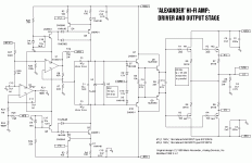
I guess this build also qualifies as 'Alexander' amp - with fet outputs:
https://www.diyaudio.com/community/threads/unusual-amp-from-1987.357369/post-6994032
https://www.diyaudio.com/community/threads/unusual-amp-from-1987.357369/post-6994032
Alexander SSM2131 Audio Power Amp PMI SSM Audio Handbook Vol 1 1990:
https://www.proaudiodesignforum.com...wer_Amp_PMI_SSM_Audio_Handbook_Vol_1_1990.pdf
https://www.proaudiodesignforum.com...wer_Amp_PMI_SSM_Audio_Handbook_Vol_1_1990.pdf
- Home
- Amplifiers
- Solid State
- The Alexander amp - current feedback and opamps