Hi i'm doing a project at tafe which involves describing an operation of an amplifier circuit we have built.
It's a design from an electronics magazine so i've had to blank out component values so it cannot be constructed without paying for the magazine etc.
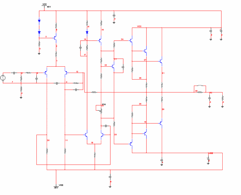
Basically I'm looking for a good way to explain how the the signal comes out of the the 2nd diff amp and is fed into the bases of the driver transistors.
Because the students are only beginners the teacher has explained to them that the bjt on the current mirror supplies an antiphase voltage to the driver at the top and the transistor below it in the diff pair supples an in phase voltage to the other driver.
Surely this amplfier doesnt need anti-phase signals? i am correct yes?
So if u have a really good way to explain this part of the circuit better please hit me back. I understand it to a degree but i still have a lot of trouble 'getting it'
thankyou
It's a design from an electronics magazine so i've had to blank out component values so it cannot be constructed without paying for the magazine etc.
Basically I'm looking for a good way to explain how the the signal comes out of the the 2nd diff amp and is fed into the bases of the driver transistors.
Because the students are only beginners the teacher has explained to them that the bjt on the current mirror supplies an antiphase voltage to the driver at the top and the transistor below it in the diff pair supples an in phase voltage to the other driver.
Surely this amplfier doesnt need anti-phase signals? i am correct yes?
So if u have a really good way to explain this part of the circuit better please hit me back. I understand it to a degree but i still have a lot of trouble 'getting it'
thankyou
Guitar-joe,
the second diff amp in the VAS is loaded with a current mirror (as you state). This is simply a high gain voltage amplifier.
The output stage is not driven 'anti-phase' and this is probably what is leading you astray.
It is the current mirror is driven 'anti-phase' by the 2nd diff amp - as one side of the 2nd diff amp pair turns on harder, the other side will turn off (as is expected in a diff amp). This is 'mirrored' by the mirror load. Why use a current mirror in this circuit and not just a resistor load? Because the current morror provides a very high effective load resistance to the 2nd diff amp, thereby increasing the stages gain. (there other advantages, but no need to cover these here).
To understand how the output stage is driven, imagine that the Vbe muliplier is shorted out. You can then see that the output halves are not driven anti-phase since both bottom and top halves would be shorted together. The amplifier still works (x-over distortion of course will be high since there is no Vbe mulitplier). As the VAS voltage swings above ground, the upper output will conduct into the load while the bottom output transistor will be off. When the VAS output then swings below 0V, the reverse happens and the top transistor turns off and the bottom one conducts.
Yes that sounds more like it.
It's probably the best way to explain it and the only way i can accept that this circuit works.
I argued the current mirror was there to ensure high gain in the second diff pair however my teacher must of thought it was too difficult a concept for the other students to understand.
If i'm not mistaken it's the reason why differential outputs are taken from the first stage in the first place, yes?
I was trying to explain how having high open loop gain is a
benefit for bandwidth and he didnt much like that either, it was too technical apparently.
If there is one thing that confuses me still it's only slight, Why is the collector of the current mirror tied to the base resistor of the driver? Is this a stability thing or is something more detailed at work here?
In conclusion i don't think less of my teacher. I know electronics is a very hard thing to teach, however i just thought his way of explaining it was detrimental to actually getting a grasp of what was really going on.
thanks for the replies
High gain is not necessarily a benefit for bandwidth, what it means is that when feedback is applied there is a lot of feedback which can be used to fight distortion.
The collector of the current mirror is tied to the base of the upper driver because the upper driver needs drive. The upper and lower drivers (and output devices) will always follow the same signal but with the bias voltage generated by the Vbe multiplier superimposed between them.
The collector of the current mirror is tied to the base of the upper driver because the upper driver needs drive. The upper and lower drivers (and output devices) will always follow the same signal but with the bias voltage generated by the Vbe multiplier superimposed between them.
*High gain is not necessarily a benefit for bandwidth, what it means is that when feedback is applied there is a lot of feedback which can be used to fight distortion.
Ok cool, basically that was the idea. If you have heaps of gain, it can be sacrifised in a closed look to flatten out the frequency response.
*The collector of the current mirror is tied to the base of the upper driver because the upper driver needs drive. The upper and lower drivers (and output devices) will always follow the same signal but with the bias voltage generated by the Vbe multiplier superimposed between them.
Ok so basically this is to give more current drive to those transistors, looking at the schematic you could say the current mirrors pole in terms of current is common to both drivers yeah?
thanks for replies i think getting there with the explanation now. cheers
The current mirror in the second diff stage actually converts the differential stage's currents to a push-pull current. So, the top half (current mirror) and bottom half (diff. stage right side) actually have oposing currents, not voltages.
How does this translate to high gain?
Immagine the VAS stage was not conencted to the drivers, so in other words, unloaded. Also, immagine the Vbe multiplier parts were omitted and the right collectors of the current mirror and LTP were directly connected.
What you have are two current sources in series - in theory, this is an impossible situation becasue current sources have infinite impedances, so even if their currents were absolutely equal, the voltage at the interconnect point would be undefined.
In reality, BJTs are not perfect current sources, but they still have very high output impedances. This means that any DIFFERENCE of the current from the current mirror and LTP right sides, acts on a very high impedance, hence only a slight difference would give a huge voltage change - in other words, a very high voltage gain.
The advantage of such a stage is threefold:
1) The gan is high because it's a current source driving a very high impedance (another current source).
2) Compared to a regular current sourced VAS, the gain is double for the same transistor current, because both sides contribute to the current change. If the LTP side pulls 1mA more current, the current mirror side pushes 1mA less current. A regular current source in it's oplace would remain constant, so the net difference would be only the 1mA, in this case it is 1-(-1)=2mA.
3) The maximum push and pull current are inherently limited, and equal the tail current of the LTP. In a regular VAS, unless extra measures are taken, the current through the VAS transistor is only limited by it's beta times the current from the first stage, this can be a rather large, and even destructive value. On the other hand, if there is a regular current source oposing it, the current in that direction is limited by the current source. As a result the maximum positive and negative currents in the regular setup are often wildly different, leading to various problems, like unequal slew rate, bad clipping recovery, and in the case of overload, even VAS transistor destruction.
In the setup above, the sink and source currents are precisely equal and limited, which avoids all of that.
The disadvantage of this setup is threefold
1) Due to minimum voltage requirements for the LTP tail, the output swing can be a bit lower than that of a regular current source terminated VAS. Without a bit of attention this usually leads to asymetrical maximum swing, and thus asymetrical clipping for the whole amp.
2) The stage inherently supresses even harmonics. In terms of raw distortion figures this can be a benefit, but in case of psychoacustics, it is not necessairly a good thing. This disadvantage is heavily debated")
3) There is extra complexity due to the doubling of components, and a thermal balancing issue, because of one side having voltage and current swing (right), while the other only has current swing (left). This must usually be remedied by yet another BJT in a cascode position between the LTP and current mirror left side, but at some expense in stability margin.
How does this translate to high gain?
Immagine the VAS stage was not conencted to the drivers, so in other words, unloaded. Also, immagine the Vbe multiplier parts were omitted and the right collectors of the current mirror and LTP were directly connected.
What you have are two current sources in series - in theory, this is an impossible situation becasue current sources have infinite impedances, so even if their currents were absolutely equal, the voltage at the interconnect point would be undefined.
In reality, BJTs are not perfect current sources, but they still have very high output impedances. This means that any DIFFERENCE of the current from the current mirror and LTP right sides, acts on a very high impedance, hence only a slight difference would give a huge voltage change - in other words, a very high voltage gain.
The advantage of such a stage is threefold:
1) The gan is high because it's a current source driving a very high impedance (another current source).
2) Compared to a regular current sourced VAS, the gain is double for the same transistor current, because both sides contribute to the current change. If the LTP side pulls 1mA more current, the current mirror side pushes 1mA less current. A regular current source in it's oplace would remain constant, so the net difference would be only the 1mA, in this case it is 1-(-1)=2mA.
3) The maximum push and pull current are inherently limited, and equal the tail current of the LTP. In a regular VAS, unless extra measures are taken, the current through the VAS transistor is only limited by it's beta times the current from the first stage, this can be a rather large, and even destructive value. On the other hand, if there is a regular current source oposing it, the current in that direction is limited by the current source. As a result the maximum positive and negative currents in the regular setup are often wildly different, leading to various problems, like unequal slew rate, bad clipping recovery, and in the case of overload, even VAS transistor destruction.
In the setup above, the sink and source currents are precisely equal and limited, which avoids all of that.
The disadvantage of this setup is threefold
1) Due to minimum voltage requirements for the LTP tail, the output swing can be a bit lower than that of a regular current source terminated VAS. Without a bit of attention this usually leads to asymetrical maximum swing, and thus asymetrical clipping for the whole amp.
2) The stage inherently supresses even harmonics. In terms of raw distortion figures this can be a benefit, but in case of psychoacustics, it is not necessairly a good thing. This disadvantage is heavily debated
3) There is extra complexity due to the doubling of components, and a thermal balancing issue, because of one side having voltage and current swing (right), while the other only has current swing (left). This must usually be remedied by yet another BJT in a cascode position between the LTP and current mirror left side, but at some expense in stability margin.
Oh, and BTW higher OLG does not necesairly translate to any benefit in bandwidth, or it's flatness.
This is because increasing OLG may come with decreasing of it's corner frequency. As a result what yiou get is only more precision (overal gain is more dependant on the feedback) towards DC, because at those frequencies there is more 'spare gain', but the bandwidth may remain the same because at higher frequencies the OLG remains the same.
In general, however, substituting a regular current source terminated VAS with ths push-pull VAS does in theory increase the OLG bandwidth becase the maximum current available from the VAS doubles due to the push-pull effect. This is important because the VAS usually drives the compensation capacitor (often somewhat imprecisely referred to as the milelr compensation capacitor), which is usually the main determinant of the OLG bandwidth. However, the phase characteristics of this added OLG may require a larger cap for stability, so in the end you may end up with the same bandwidth again.
- Status
- This old topic is closed. If you want to reopen this topic, contact a moderator using the "Report Post" button.
- Home
- Amplifiers
- Solid State
- Explaining the operation of a VAS in this amp