#347
May I consider this schematic as a balanced connection of the JC-3? If not, what should be the correct balanced connection?
May I consider this schematic as a balanced connection of the JC-3? If not, what should be the correct balanced connection?
Looking good, Mike!
Glad you added the compensation caps")
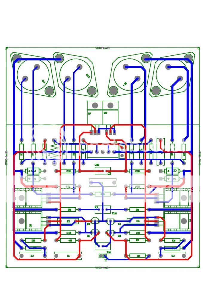
Attached is a brdiged version of JC-3.
Will post distorion sweeps later this week.
Sigurd
Last edited:
Hi Patrick
Very nice schematic but no parts values. What would be the current for the 1st stage? 8ma from post 347 or more current is needed?
Very nice schematic but no parts values. What would be the current for the 1st stage? 8ma from post 347 or more current is needed?
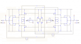
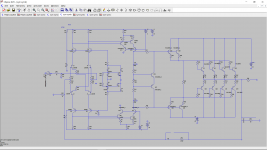
If I were to do a balanced JC-3, then this is probably what I would do.
Schematics is simplified to illustrate principle.
But of course you should really ask John himself.
Cheers,
Patrick
.
Last edited:
I understand what you meant, if the SE circuit works, then this balanced circuit will work but maybe needs revised current for each stage.
As said, the schematics is only to demonstrate how to turn the original SE circuit to balanced.
Patrick
The values has too bee calculated dependent on what you choose as operating points and so on..... Hence the original circuit and todays transistors require slightly different compensations. So to ask abt values you start with original values. in this simplified input and vas in a ballanced / bridgevariation you can start with original values.
Different jfets require differens values as input stage differencial currens varies with values of passive and choice of active components and their choosen working points. And then how you choose to compensate this circuit with todays aktiva may wary slightly from components about 30 years ago.
Original values vas somthing close to 10 Ohms to rails and 220 Ohms to base of Vamp transistors. The gain in shown circ may bee on the high side, som sorce resistance on the jfets may bee considered.
Enjoy the fun !
Attachments
The values has too bee calculated dependent on what you choose as operating points and so on..... Hence the original circuit and todays transistors require slightly different compensations. So to ask abt values you start with original values. in this simplified input and vas in a ballanced / bridgevariation you can start with original values.
Different jfets require differens values as input stage differencial currens varies with values of passive and choice of active components and their choosen working points. And then how you choose to compensate this circuit with todays aktiva may wary slightly from components about 30 years ago.
Original values vas somthing close to 10 Ohms to rails and 220 Ohms to base of Vamp transistors. The gain in shown circ may bee on the high side, som sorce resistance on the jfets may bee considered.
Enjoy the fun !
Hi Dijk, thank you for your reply. I will start with the original parts & value and let's see what is gonna happen.
Hi sir, Ive made a few "nearly" original.If I were to do a balanced JC-3, then this is probably what I would do.
Schematics is simplified to illustrate principle.
But of course you should really ask John himself.
Cheers,
Patrick
.
But if i where to make som PCB's i had left the option to kaskode the vas stage.
And if i went for it i would like the option for kaskode input stage as well.
In this possibillity there vould easy become a second output at the unused grounded kaskodetransistors in vas stage.
Second i would love a simple regulation for input stage powersupply please.
For thouse really advanced the P and N every other on output stage cooling for heat and current distribution.
So IF this is a wishlist.... a simple j-fet buffer somthing that may bee just perfect for one phase buffer for the ballanced input maybee the idea came from ML2 ?
Hope you enjoy it cause i do
Attachments
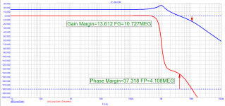
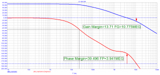
The frequency of the first pole without nested feedback loops is higher than the audio range, so it is quite possible to reduce the depth of nested feedbacks and transfer more "authority" to the overall feedback
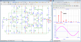
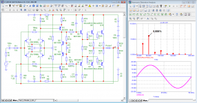
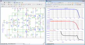
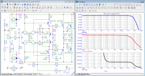
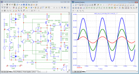
This is what comes out of this during the simulation.
This is what comes out of this during the simulation.
Attachments
After reviewing the 1999 interview and the 2006 recommendations of John Curl, the following conclusions can be drawn:
- to date, no type of testing correlates with sound quality (cannot predict sound quality);
- practical experience in designing and listening to finished products speaks in favor of amplifiers having a high first pole before being covered by general negative feedback. the first pole above the audio range guarantees constant output impedance and harmonic distortion in the audio band, as well as low phase distortion. Output impedance in phase with external influences. This was proved in his works by Matti Otala; This approach to design guarantees high speed parameters: low signal transit time (no more than 100 ns), high slew rate of the output voltage (SR> = 100 V / uS);
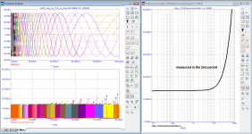
- low speed distortions (distortions of the first period (FCD) according to Graham Maynard);
- the amplifier must have a low output impedance even before being covered by the general negative feedback and have a high load capacity to overcome the back EMF of the loudspeakers. For this purpose, the output transistors are paired beforehand by carefully selecting them according to their parameters so that they "sing" in a coordinated "chorus".
Based on the recommendations of John Curl, an amplifier model was developed with the following parameters:
- full power bandwidth over 1 MHz; the rate of rise of the output voltage is not less than 200 V / μs;
- the level of harmonics of the first period at a frequency of 20 kHz is not more than minus 90 dB (0.003%);
- the signal transit time is 73 ns (tPD = 73 nS);
- servo control system is able to compensate for DC input voltage up to + -0.5 V;
- quiescent currents of output transistors (including field ones) 110 ± 10 mA each;
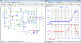
- output impedance Rout = 12 mOhm (0.012 Ohm). Dumping factor = 8 / 0.012 = 470. The growth of the output impedance begins above 100 kHz.
- thanks to the buffered cascade at the input, the amplifier is not whimsical to the output impedance of the signal source
regards
Petr
- to date, no type of testing correlates with sound quality (cannot predict sound quality);
- practical experience in designing and listening to finished products speaks in favor of amplifiers having a high first pole before being covered by general negative feedback. the first pole above the audio range guarantees constant output impedance and harmonic distortion in the audio band, as well as low phase distortion. Output impedance in phase with external influences. This was proved in his works by Matti Otala; This approach to design guarantees high speed parameters: low signal transit time (no more than 100 ns), high slew rate of the output voltage (SR> = 100 V / uS);
- low speed distortions (distortions of the first period (FCD) according to Graham Maynard);
- the amplifier must have a low output impedance even before being covered by the general negative feedback and have a high load capacity to overcome the back EMF of the loudspeakers. For this purpose, the output transistors are paired beforehand by carefully selecting them according to their parameters so that they "sing" in a coordinated "chorus".
Based on the recommendations of John Curl, an amplifier model was developed with the following parameters:
- full power bandwidth over 1 MHz; the rate of rise of the output voltage is not less than 200 V / μs;
- the level of harmonics of the first period at a frequency of 20 kHz is not more than minus 90 dB (0.003%);
- the signal transit time is 73 ns (tPD = 73 nS);
- servo control system is able to compensate for DC input voltage up to + -0.5 V;
- quiescent currents of output transistors (including field ones) 110 ± 10 mA each;
- output impedance Rout = 12 mOhm (0.012 Ohm). Dumping factor = 8 / 0.012 = 470. The growth of the output impedance begins above 100 kHz.
- thanks to the buffered cascade at the input, the amplifier is not whimsical to the output impedance of the signal source
regards
Petr
Attachments
-
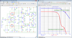
 AMP_Like_JC_Bode.png89.9 KB · Views: 82
 -
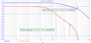 AMP_Like_JC_Loop-Gain.png31.2 KB · Views: 84
 -
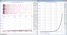
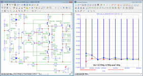 AMP_Like_JC_20kHz-FCD.png82.2 KB · Views: 71
 -
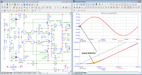 AMP_Like_JC_Speed-dist.png87.9 KB · Views: 65
 -
 AMP_Like_JC_Rout_Bode.png81.8 KB · Views: 60
 -
 AMP_Like_JC_AH-1MHz.png84.9 KB · Views: 69
 -
 AMP_Like_JC_THD_vs_Freq.png86.5 KB · Views: 71
The need for high open loop bandwidth and very low open loop output impedance were disproven many years ago.
That having been said, high slew rate and high open-loop linearity are important. High output current drive and an amplifier with low closed loop output impedance improve sound quality. Damping factor should be high, but it need not be flat with frequency as long as it is high. For example, it is fine if an amplifier has a damping factor of 1000 at DC that falls to 50 at 20 kHz.
Most of Otala's claims concerning TIM, IIM and PIM were disproven long ago. Large amounts of negative feedback do not increase these distortions in a properly designed amplifier. These distortions are objectively measurable and have been shown to be usually in fact smaller in amplifiers with large amounts of negative feedback.
Otala deserves credit for bringing these distortions to people's attention AND for developing tests for measuring them. However, his own tests, all of which I have carried out, showed that his thesis that high negative feedback and low open-loop bandwidth was wrong.
Cheers,
Bob
I consider 50 V/us plenty adequate for a 100-w amplifier.
However, it is not just about raw slew rate alone. When you hit the slew rate limit, that is like clipping in the time domain. One can still have significant rising distortion before the slew rate limit is hit. Some have referred to this as "soft TIM" or "soft slewing induced distortion". This is often the result of nonlinearities in the input stage that cause rising high-frequency distortion well before the input stage runs out of current.
There are also some amplifiers that achieve high slew rate by allowing the input stage to exit the class A region and still provide the needed charging current in either polarity. This is more often the case with some current feedback amplifiers. This mode of operation can cause some distortion in the same way that a class AB output stage causes distortion as opposed to a class A output stage. I believe that when high slew rate is achieved at the expense of pure class A input stage or VAS operation, that does not necessarily improve matters.
One might say that high slew rate is necessary but not sufficient in order to achieve low levels of high-frequency distortion.
Cheers,
Bob
- Home
- Amplifiers
- Solid State
- John Curl amp