Hi,
Since building a pair of Hitachi / Maplin Lateral MOSFET amps in 2001, they have been faultless ever since. I have four of these amps, both with the CCS mods.
The amp is based around the Hitachi lateral mosfet apps data, but with added Constant Current Sources, up-rated to run at +/-70v. I would love to post the schematic, but the mods are copyrighted by someone I no longer have contact with (the amp retains the Maplin topology, but uses a CCD to the emitters of the Input LTP and a Constant Current Source to prevent rail sag affecting the Current Mirror).
Up until I added the extra mosfets, which has resulted in the situation I see now, the amp was running just 1 x 16A N-ch + 1 x 16A P-ch Exicon Lateral Mosfet. I've now gone for 4 x P and 4 x N (amps are fully dual-mono).
The mosfets are from sequential production(the kind of issue I have isn't matching related to my knowledge...).
I build the first amp... Bingo! It can sustain up to 3A bias without oscillating. DC offset less than 15mV at outputs.
I build 2nd amp... -32v DC at output... Increasing Gate Resistors seems to make the problem worse! Unfortunately, my 50Meg ‘scope isn’t working, and I can’t even see a blur on my 20Meg ‘scope. Zobel resistor isn’t hot btw.
I wonder if there’s an issue with the VAS, so I swap it against the VAS from the good amp: the working mosfet banks (N+P) are fine with the other VAS, and the bad MOSFET banks won’t work with the other VAS.
As I have a working amp and have swapped the VAS over, I ordered some more mosfets and assumed it was an issue there... New mosfets behave the same…
I match a quad of N-ch mosfets for Vgs and try them – same -32v DC
When I turned on the amp with a +/-50v supply by accident, without any n-ch connections at all (no Gate. Source or Drain), I got -32v DC…coincidence?
There is no voltage between the N-ch and P-ch Gates...v odd. (about 20mV)
The bias trimmer on the problem amp is really non-linear; whereas it’s progressive with the working amp (25 turn pot), it seems to jump from 200mA to 1A bias without warning…almost as if a parasitic oscillation has been triggered….
The amp doesn’t tolerate having a dummy load connected to its output (-32v DC).
The thing that I find puzzling is that the working MOSFET bank works fine with either VAS, with minimal DC offset…
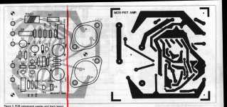
Because the Maplin PCB only has provision for 1 x N-ch and 1x P-ch, I have sawn the PCB off where you see the redline (see attachment). 1.25mm copper wire is used for the Source wiring – it comes off the PCB track and connects to the cases via M3 solder tags.
I can stop the oscillation if I put the MOSFETs back in the place they’re meant to go, still via 1.25mm wire, but with minimal wiring… I can only conclude that my wiring is at fault here… As I’ve included the PCB, I would like to ask: how would you attach the parallel MOSFETs? The Maplin manual shows a diagram illustrating how easy it is to parallel MOSFETs, but doesn’t say how they should be wired…is 1.25mm solid wire too thin?
One idea is to common all the Sources via a heat-transfer bracket, but I don’t know how you’d do that as silicone compound is needed to ensure thermal transfer, which will compromise the quality of connection…how do you do that one? Currently, I have them insulated on a heatsink.
BTW – I’m not after opinions on the sound of the Maplin amps!
Many thanks in advance.
Justin
Since building a pair of Hitachi / Maplin Lateral MOSFET amps in 2001, they have been faultless ever since. I have four of these amps, both with the CCS mods.
The amp is based around the Hitachi lateral mosfet apps data, but with added Constant Current Sources, up-rated to run at +/-70v. I would love to post the schematic, but the mods are copyrighted by someone I no longer have contact with (the amp retains the Maplin topology, but uses a CCD to the emitters of the Input LTP and a Constant Current Source to prevent rail sag affecting the Current Mirror).
Up until I added the extra mosfets, which has resulted in the situation I see now, the amp was running just 1 x 16A N-ch + 1 x 16A P-ch Exicon Lateral Mosfet. I've now gone for 4 x P and 4 x N (amps are fully dual-mono).
The mosfets are from sequential production(the kind of issue I have isn't matching related to my knowledge...).
I build the first amp... Bingo! It can sustain up to 3A bias without oscillating. DC offset less than 15mV at outputs.
I build 2nd amp... -32v DC at output... Increasing Gate Resistors seems to make the problem worse! Unfortunately, my 50Meg ‘scope isn’t working, and I can’t even see a blur on my 20Meg ‘scope. Zobel resistor isn’t hot btw.
I wonder if there’s an issue with the VAS, so I swap it against the VAS from the good amp: the working mosfet banks (N+P) are fine with the other VAS, and the bad MOSFET banks won’t work with the other VAS.
As I have a working amp and have swapped the VAS over, I ordered some more mosfets and assumed it was an issue there... New mosfets behave the same…
I match a quad of N-ch mosfets for Vgs and try them – same -32v DC
When I turned on the amp with a +/-50v supply by accident, without any n-ch connections at all (no Gate. Source or Drain), I got -32v DC…coincidence?
There is no voltage between the N-ch and P-ch Gates...v odd. (about 20mV)
The bias trimmer on the problem amp is really non-linear; whereas it’s progressive with the working amp (25 turn pot), it seems to jump from 200mA to 1A bias without warning…almost as if a parasitic oscillation has been triggered….
The amp doesn’t tolerate having a dummy load connected to its output (-32v DC).
The thing that I find puzzling is that the working MOSFET bank works fine with either VAS, with minimal DC offset…
Because the Maplin PCB only has provision for 1 x N-ch and 1x P-ch, I have sawn the PCB off where you see the redline (see attachment). 1.25mm copper wire is used for the Source wiring – it comes off the PCB track and connects to the cases via M3 solder tags.
I can stop the oscillation if I put the MOSFETs back in the place they’re meant to go, still via 1.25mm wire, but with minimal wiring… I can only conclude that my wiring is at fault here… As I’ve included the PCB, I would like to ask: how would you attach the parallel MOSFETs? The Maplin manual shows a diagram illustrating how easy it is to parallel MOSFETs, but doesn’t say how they should be wired…is 1.25mm solid wire too thin?
One idea is to common all the Sources via a heat-transfer bracket, but I don’t know how you’d do that as silicone compound is needed to ensure thermal transfer, which will compromise the quality of connection…how do you do that one? Currently, I have them insulated on a heatsink.
BTW – I’m not after opinions on the sound of the Maplin amps!
Many thanks in advance.
Justin
Attachments
Hi Trev,
I've tried a variety of Gate Stopper methods; single resistors up to 330R and the Randy Sloane method, where you put resistors on each Gate terminal, with them all fed from an extra resistor.
I powered up 4 banks of N+P and shut them down individually to see how many would be running * if * the oscillation stopped... It didn't...even with just 1 x N / 1 x P.
However, when I put just 1 x N / 1 x P in the same space allocated for the original MOSFETs, fed with 1.25mm wire instead of the PCB which I chopped, all was fine and perfect Class B operation ensued (i.e. current draw went up as oscillator level increased and bias pot was predictable).
With the MOSFETs in the original place, all leads are less than 1" - my problem is trying to figure out how to emulate this with 4 banks of each type...
The most frustrating thing is having one perfect amp...both amps are identical, but the second one won't play ball with any MOSFETs, unless I remove the VAS and couple a pair as they would be in the original amp.
Thanks,
Justin
The next thing I would try is a source resistor 0.5 ohm on each device! I know this is not normally recomended but its worth a try !
Then the next thing I would try is some low value caps around the vas stage you may be on the verge of instability !!
However without the schematic its not so easy to see what his happening
regards Trev
Then the next thing I would try is some low value caps around the vas stage you may be on the verge of instability !!
However without the schematic its not so easy to see what his happening
regards Trev
you can get strip line effects when paralleling lateral mosfets,
and this can cause problems in the drive decupling as well as the feed back
i run upto 8 pairs in parralel and there is skill in building hi power
fet amps
also some batches of fets will differ in stability
andy
and this can cause problems in the drive decupling as well as the feed back
i run upto 8 pairs in parralel and there is skill in building hi power
fet amps
also some batches of fets will differ in stability
andy
Read Troy Heubner's Application Note 1645 from national semiconductor -- you will find it in the product folder for the LM4702 -- he discusses the gate stopper resistors. you select based upon the input capacitance of the MOSFETs --
i have paralleled Matched Renesas and Hitachi Lateral MOSFETs with 0.1R Source Resistors. 0.5R wastes a lot of power.
i have paralleled Matched Renesas and Hitachi Lateral MOSFETs with 0.1R Source Resistors. 0.5R wastes a lot of power.
Thank you very much to all!
I have been reading this article on MOSFET implementation: http://documentation.renesas.com/eng/products/transistor/rej27g0017_charalterstics.pdf
The article suggested by Jack is the most comprehensive one I've found on Rgate values - thanks: http://www.national.com/an/AN/AN-1645.pdf#page=1
What is so frustrating is that I have a working amp, yet the identical one doesn't want to play ball however I wire it... (excuse me for repeating my frustration!)
It does appear to be my layout as I can get the new MOSFETs to work if I put them less than an inch from the Source track on the PCB...it's when I put them into a 'real world' arrangement a few inches away, connected via 1.25mm solid wire that they play up...
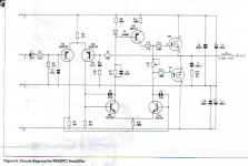
I've attached a schem for the amp. Note that the 47R resistor going to the LTP emitters is replaced with a CCD and R9 is replaced by a CCS. Some resistor values are uprated for higher voltage operation and the Current Mirror driver transistors are replaced with Hitachi BJTs for higher voltage operation and extra drive.
Funnily enough, when I compared the uprated amp to a standard Maplin one, I found it's less prone to oscillation and seems to work better in general, so I don't think the culprit here is in the VAS at all - purely down to my implementation of the MOSFETs...
I took the liberty of asking Bruno Putzeys at his forum about this issue... He was highly critical of the stability of Lateral MOSFETs and told me he prefers to replace them with IRF devices...
Justin
I have been reading this article on MOSFET implementation: http://documentation.renesas.com/eng/products/transistor/rej27g0017_charalterstics.pdf
The article suggested by Jack is the most comprehensive one I've found on Rgate values - thanks: http://www.national.com/an/AN/AN-1645.pdf#page=1
What is so frustrating is that I have a working amp, yet the identical one doesn't want to play ball however I wire it... (excuse me for repeating my frustration!)
It does appear to be my layout as I can get the new MOSFETs to work if I put them less than an inch from the Source track on the PCB...it's when I put them into a 'real world' arrangement a few inches away, connected via 1.25mm solid wire that they play up...
I've attached a schem for the amp. Note that the 47R resistor going to the LTP emitters is replaced with a CCD and R9 is replaced by a CCS. Some resistor values are uprated for higher voltage operation and the Current Mirror driver transistors are replaced with Hitachi BJTs for higher voltage operation and extra drive.
Funnily enough, when I compared the uprated amp to a standard Maplin one, I found it's less prone to oscillation and seems to work better in general, so I don't think the culprit here is in the VAS at all - purely down to my implementation of the MOSFETs...
I took the liberty of asking Bruno Putzeys at his forum about this issue... He was highly critical of the stability of Lateral MOSFETs and told me he prefers to replace them with IRF devices...
Justin
Attachments
One option I have yet to try is fitting Capacitors between Gate and Source. I've seen this on a few versions of Hitachi amp and it was also suggested to me by someone with experience on the Exicon MOSFETs.
BTW - Can someone explain to me why I would need Source resistors? I was under the impression they were needed either to prevent Thermal Runaway (not an issue with Lateral MOSFETs) or to provide a voltage for protection circuitry sensing - what other benefits do they have?
Thanks.
J
BTW - Can someone explain to me why I would need Source resistors? I was under the impression they were needed either to prevent Thermal Runaway (not an issue with Lateral MOSFETs) or to provide a voltage for protection circuitry sensing - what other benefits do they have?
Thanks.
J
Hi,
that schematic shows the FETs driven directly by the VAS.
This is not a good arrangement.
The high output impedance from the VAS fights against the low source impedance required by the FETs.
One normally sees a pair of EF drivers between VAS and FETs.
The high output impedance of the VAS could be exaggerating the instability problem with the FETs. In addition, the 4pair have 4times the transconductance of a single pair. This extra voltage to current amplification can also give rise to instability.
As for one amp working and one not, that could be explained by the last paragraph to follow.
Since you are separating the voltage amp from the FETS, can you squeeze a couple of complementary drivers into the spare PCB space vacated by the FETS?
All the voltage tappings for the drivers are there and you would only have to tack on a single or pair of emitter resistors between the drivers.
The FETs vary in voltage between each other far more than BJTs. to get better matching over a range of currents the source resistor absorb some of the difference in Vgs when the currents become unbalanced between the Nsets or the Psets.
At low drive voltages the source resistor has less effect and here accurate matching of Vgs at the operating currents are far more important.
At higher output currents the volts drop across the source resistor becomes ever more significant.
Match the source resistors to better than 1%.
Match the Vgs to better than 10mV.
You have 4pair in 4amps. That's 16pair. You should be able to group your FETs into sets of 4 and hopefully there will be less than 10mV between top and bottom in each set.
AndrewT said:
Match the Vgs to better than 10mV.
You have 4pair in 4amps. That's 16pair. You should be able to group your FETs into sets of 4 and hopefully there will be less than 10mV between top and bottom in each set.
From the statistical analysis I have done matching HexFets and Lateral MOSFETs I would say you need about 300 devices if you want to match 4 sets of 4 to better than 10 mV. EDIT: I set out 300 to 500 devices at a time, remove them from their packaging tubes and let them come to temperature -- usually an hour or so -- when I measure the devices I almost always get a bimodal distribution of Vgs values, and the distribution is not completely normal -- i.e. you have somewhat fat tails. Interestingly, the last time I regressed the transconductance with Vgs for devices from the same lot gm was tightly correlated. This could change as Vishay takes over from IRF.
Going from unmatched to matched lateral MOSFET's in my LM4702 amplifier brought the THD to 0.0014%.
With regard to Lateral MOSFET stability, it seems that its only an issue when you try to get the slew rate way up. You can make HexFets behave badly as well.
Hi Jack,
I have previously reported my test results in matching 16pair of 1058/162 laterals into sets of four.
7sets were well within 10mV and one set had three close and the fourth was slightly outside my tolerance.
I reported the effect of this low Vgs cf it's three partners.
I do not have access to 300 FETs. I just ordered up 16 pair from Rapid online (before they reduced their prices by 30% )
)
Maybe I was lucky. But more likely, if I had ordered 20pair I could have got significantly better than <10mV in each set of 4 and had 4pair unmatched for other uses.
I have previously reported my test results in matching 16pair of 1058/162 laterals into sets of four.
7sets were well within 10mV and one set had three close and the fourth was slightly outside my tolerance.
I reported the effect of this low Vgs cf it's three partners.
I do not have access to 300 FETs. I just ordered up 16 pair from Rapid online (before they reduced their prices by 30%
)Maybe I was lucky. But more likely, if I had ordered 20pair I could have got significantly better than <10mV in each set of 4 and had 4pair unmatched for other uses.
AndrewT said:
that schematic shows the FETs driven directly by the VAS.
This is not a good arrangement.
Hi Andrew,
You have to be careful with statements like that.
The design may not be optimum but you have to remember that this design was published in the Maplin magazine and reviewed again, years on.
The design was also sold both as a kit and as ready-built. Thousands were made or sold. I have six with no problems at all.
Had there been any problems, you can bet that this would have been fed back to Maplin and the design would have been modded.
Justin,
It may help if you post a photo of each channel so we can compare them. Identical may not be so.
Andy
As an aside, I recall the Rod Elliot wrote about his P101 that it took many iterations and revision over a year to get the PCB layout working right and that just looking at the schematic was not enough. I mention this as a kind of cheer leading -- apparently getting parallel L-MOSFETS to operate the way you want is not a piece of cake. So don't get discouraged.
AndrewT said:that schematic shows the FETs driven directly by the VAS.
This is not a good arrangement.
The high output impedance from the VAS fights against the low source impedance required by the FETs.
One normally sees a pair of EF drivers between VAS and FETs.
The high output impedance of the VAS could be exaggerating the instability problem with the FETs.
I stand by my statement.poynton said:You have to be careful with statements like that.
The design may not be optimum but you have to remember that this design was published in the Maplin magazine and reviewed again, years on.
The design was also sold both as a kit and as ready-built. Thousands were made or sold. I have six with no problems at all.
Had there been any problems, you can bet that this would have been fed back to Maplin and the design would have been modded.
There have been numerious reports and technical/performance discussion on the error of trying to drive FETs directly from the VAS.
This is not a good arrangement.
It may be adequate for a low cost, low quality magazine design but that Maplin did not increase the transistor count by two, does not and never can make it good.
And no, I will not take your bet, I am liable to lose.
differant batches have diferent behavior with semilab lateral fets.
I know i have used 100@s off thousands off them.
and even these days the Hitatchi fets can be different from batch to batch.
also the semilab lateral fets are not the same as the hitatchi!
this can show itself with instability.
I know i have used 100@s off thousands off them.
and even these days the Hitatchi fets can be different from batch to batch.
also the semilab lateral fets are not the same as the hitatchi!
this can show itself with instability.
There have been numerious reports and technical/performance discussion on the error of trying to drive FETs directly from the VAS.
This is not a good arrangement.
Did any of those reports mention the ESP P101? If so, I would be curious to see if R.E. has a response.
thermionic said:One option I have yet to try is fitting Capacitors between Gate and Source. I've seen this on a few versions of Hitachi amp and it was also suggested to me by someone with experience on the Exicon MOSFETs.
BTW - Can someone explain to me why I would need Source resistors? I was under the impression they were needed either to prevent Thermal Runaway (not an issue with Lateral MOSFETs) or to provide a voltage for protection circuitry sensing - what other benefits do they have?
Thanks.
J
sam9 said:
Did any of those reports mention the ESP P101? If so, I would be curious to see if R.E. has a response.
The ESP P101 has both the caps and the resistors.
Andy
hi there,
the good old maplin/hitachi mosfet module, i have built loads of these including adding extra parralel mosfets to them.
i found that now and then there would be a rouge, instability going into buseniss in the RF band for its self.
things i found to do with them was
make sure the resistor in the zobel is not wirewound, check the cap in the zobel is still alive wilst your at it.
bypass the electroytic in the feed back with 10n.
make sure chassis, heatsinks/mounting brackets are grounded including the extra pairs of course.
bypass as near to the devicies as possible with 100u and 100n on each rail.
keep extra mosfet wiring short, point to point is best
twist the power supply wires from smoothing cap's to pcb, twist the speaker wires along there lenth.
i had a couple of these modules that were particularly troublesome in this regard, even after swopping bits and all the above, these were cured strange as it may seem by taking the speaker returns (-) directly to the pcb, rather than the smoothing cap star point.
hope this helps
bob
- Status
- This old topic is closed. If you want to reopen this topic, contact a moderator using the "Report Post" button.
- Home
- Amplifiers
- Solid State
- How to Parallel Lateral MOSFETs...