As many readers of Doug Self's articles and books are aware, the editing of Self's publications leaves a little to be desired...Ok, it sucks!
I thought I would start a thread as a common base to list these errors for Self and his publishers, in the oft chance that they would actually DO something about them, as many of the errors are carried over from his articles and prior editions.
This may also be a home base for gaining some clarity about some of his topics.
I hope that this can be a constructive dialog for the purposes expressed above, instead of yet another drawn out subjectivist bashing.
Vbe multiplier
I noticed inconsistencies between the "Thermal Dynamics in Audio Power" article in 10/96 issue of Electronics World, and the "Audio Power Amplifier Design Handbook", 4th ed.
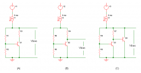
First, I noticed the same editing errors in each. Table 1 of the article and Table 13.4 of the 4th edition of the book show inconsistent values from the Figures. The values of R1 and R2 appear reversed for the EF, and R3 appears to be reversed between the EF and CFP. I assume the figures are correct.
But what is more important is that in the article, the output of the Vbe in the article is taken at the lower end of R3, as shown in (A) of the attached figure, while in the book, it is taken at the upper end of R3, as shown in (B) of the attachment. I am not sure which one is correct.
I'm guessing that the book is the correct one, because he says that the intent of R3 is to subtract a correction voltage due to current changes.
However, in (C) of the attachment, Self shows a two transistor version of Figure 13.32 of his book, where the Vbe output is again taken at the top of the resistor.
Can anyone shed any light on this issue?
Does anyone have any practical experience with this two transistor circuit regarding oscillation problems or other consequences? Would R3 also be 1k for an EF output stage?
I noticed inconsistencies between the "Thermal Dynamics in Audio Power" article in 10/96 issue of Electronics World, and the "Audio Power Amplifier Design Handbook", 4th ed.
First, I noticed the same editing errors in each. Table 1 of the article and Table 13.4 of the 4th edition of the book show inconsistent values from the Figures. The values of R1 and R2 appear reversed for the EF, and R3 appears to be reversed between the EF and CFP. I assume the figures are correct.
But what is more important is that in the article, the output of the Vbe in the article is taken at the lower end of R3, as shown in (A) of the attached figure, while in the book, it is taken at the upper end of R3, as shown in (B) of the attachment. I am not sure which one is correct.
I'm guessing that the book is the correct one, because he says that the intent of R3 is to subtract a correction voltage due to current changes.
However, in (C) of the attachment, Self shows a two transistor version of Figure 13.32 of his book, where the Vbe output is again taken at the top of the resistor.
Can anyone shed any light on this issue?
Does anyone have any practical experience with this two transistor circuit regarding oscillation problems or other consequences? Would R3 also be 1k for an EF output stage?
Attachments
Two-pole compensation
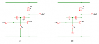
Another question I have about Self's book is his two-pole compensation diagram of Figure 7.1d on page 188 of the 4th ed.
It is reproduced in (A) of the attached figure.
He shows one end of Rp attached to the negative rail. He also states "at HF, Cp2 has low impedance and allows Pr to directly load the VAS collector to ground..." on page 193.
Thus, it would appear that Rp should be attached to ground as shown in (B) of the attachment, rather than the voltage rail as shown in (A).
Moreover, one of Self's references to two-pole compensation here shows the resistor connected to ground.
So am I correct that (B) is the correct way to do this?
This would appear to be a good way to extend the open-loop bandwidth. Does anyone have any experience with this as far as stability issues or other disadvantages? It there a way of damping the rise in open-loop at high frequencies?
Attachments
Pooge,
Regarding your first question (VBE-multipliers), B is the correct configuration. That VBE-multiplier topology has three connection nodes in oppose to two. You can simulate all three configurations (conventional and the ones without extra resistor and transistor) and see how they differ from each other if you feed the collectors with a steadily rising current. The two-transistor version, with the added resistor, stays very linear after a certain point but is in my experience just too unstable.
Regarding your first question (VBE-multipliers), B is the correct configuration. That VBE-multiplier topology has three connection nodes in oppose to two. You can simulate all three configurations (conventional and the ones without extra resistor and transistor) and see how they differ from each other if you feed the collectors with a steadily rising current. The two-transistor version, with the added resistor, stays very linear after a certain point but is in my experience just too unstable.
Thanks.
If (B) is correct, and is used in a complimentary VAS, what would be the effect of R4 on the signal? R4 is between the output of the upper VAS and the upper bias voltage. There is no corresponding resistor between the lower bias voltage and the lower VAS output.
Does this matter to the signals, or should another like resistor be placed in the lower half?
No need for another resistor. The whole VBE-multiplier as is can safely be in between the complementary VAS stages - it's the injection points to drivers/output transistors you need to worry about. You want to create a steady bias voltage between the bases of the drivers/output transistors - not in between the VAS stages. The schematic diagrams of Self's book show pretty clearly the take-off points for the bias voltage. I think this is pretty self-explanatory once you think it for a moment.
The effects of using both VBE-multiplier circuit variations are explained quite well in Chapter 12 of Self's Audio Power Amplifier Design Handbook, Third Edition. See "Current compensation", pages 362 - 364. Especially examine the figure 12.33 of the concerned book. Also, you can run the SPICE simulation I mentioned and see the effects yourself. IMO, you can visualize how the circuits work much better if you simulate them. Self's book just tells why they do what they do.
The effects of using both VBE-multiplier circuit variations are explained quite well in Chapter 12 of Self's Audio Power Amplifier Design Handbook, Third Edition. See "Current compensation", pages 362 - 364. Especially examine the figure 12.33 of the concerned book. Also, you can run the SPICE simulation I mentioned and see the effects yourself. IMO, you can visualize how the circuits work much better if you simulate them. Self's book just tells why they do what they do.
Re: Two-pole compensation
Either way would work. By "ground" he would mean "AC ground". The supply rails are at "AC ground" beacause they are bypassed.
Cheers,
Glen
pooge said:Another question I have about Self's book is his two-pole compensation diagram of Figure 7.1d on page 188 of the 4th ed.
It is reproduced in (A) of the attached figure.
He shows one end of Rp attached to the negative rail. He also states "at HF, Cp2 has low impedance and allows Pr to directly load the VAS collector to ground..." on page 193.
Thus, it would appear that Rp should be attached to ground as shown in (B) of the attachment, rather than the voltage rail as shown in (A).
Moreover, one of Self's references to two-pole compensation here shows the resistor connected to ground.
So am I correct that (B) is the correct way to do this?
Either way would work. By "ground" he would mean "AC ground". The supply rails are at "AC ground" beacause they are bypassed.
Cheers,
Glen
Re: Re: Two-pole compensation
Thanks. I was thinking he should have said signal common when connecting to the rail, since it is a common emitter. But your analysis makes sense.
G.Kleinschmidt said:
Either way would work. By "ground" he would mean "AC ground". The supply rails are at "AC ground" beacause they are bypassed.
Cheers,
Glen
Thanks. I was thinking he should have said signal common when connecting to the rail, since it is a common emitter. But your analysis makes sense.
Regarding the Vbe configurations:
I've used both B and C as opposed to just simulating them with an EF output section. Both function. My instrumentation isn't sufficient (hobby budget) to unambiguously say one or the other results in lower THD or better thermal tracking. C is harder to set but not impossible; you just need patience.
This is not a definitive evaluation but rather a recounting of practical experience of a hobbyist with limit resources.
Regarding two pole compensation:
I believe A is correct. Maybe B will work as well. The affect of A was within my means to detect and it definitely reduces THD at higher frequencies. Choosing the wrong value of Rp can cause some oscillation problems but I found you have quite a bit of latitude which may depend on the rest of the amp.
I believe A is correct. Maybe B will work as well. The affect of A was within my means to detect and it definitely reduces THD at higher frequencies. Choosing the wrong value of Rp can cause some oscillation problems but I found you have quite a bit of latitude which may depend on the rest of the amp.
Pooge,
I've ended up using the two transistor Vbe multiplier in 'C', but the main pass transistor Q4 is a PNP and not an NPN as shown in your diagram. The R7 load on Q3 is 1k.
I have a 0.1uF connected from the collector to base of the Q3 and a 10uF across the emmiter and base Q4. I have had no instability problems - this Vbe multiplier is very stable and the output resistance is low. This is important in fully symmetrical designs where the VAS current is not neccessarily constant, as opposed to current source loaded VAS topologies.
Its important that the sense transistor is correctly positioned for best thermal compensation. Self seems to make a meal out of the mechanical and thermal coupling of the Vbe multiplier. I used an SMD transistor for Q3 and I've mounted it close to the collector lead of the main output transistor so the response is quick and it s pretty stable (c. 20% total Iq variation from cold to full warm-up after playing loud music). My amp runs with high Iq of 80 - 100mA per pass transistor.
Re: Vbe multiplier
You really need to read the text to get the context. R4 is there to modify the temp tracking of the Vbe multiplier. Figs a, b and c are different ways to take care of the temp tracking.
Jan Didden
pooge said:I noticed inconsistencies between the "Thermal Dynamics in Audio Power" article in 10/96 issue of Electronics World, and the "Audio Power Amplifier Design Handbook", 4th ed.
First, I noticed the same editing errors in each. Table 1 of the article and Table 13.4 of the 4th edition of the book show inconsistent values from the Figures. The values of R1 and R2 appear reversed for the EF, and R3 appears to be reversed between the EF and CFP. I assume the figures are correct.
But what is more important is that in the article, the output of the Vbe in the article is taken at the lower end of R3, as shown in (A) of the attached figure, while in the book, it is taken at the upper end of R3, as shown in (B) of the attachment. I am not sure which one is correct.
I'm guessing that the book is the correct one, because he says that the intent of R3 is to subtract a correction voltage due to current changes.
However, in (C) of the attachment, Self shows a two transistor version of Figure 13.32 of his book, where the Vbe output is again taken at the top of the resistor.
Can anyone shed any light on this issue?
Does anyone have any practical experience with this two transistor circuit regarding oscillation problems or other consequences? Would R3 also be 1k for an EF output stage?
pooge said:Thanks.
If (B) is correct, and is used in a complimentary VAS, what would be the effect of R4 on the signal? R4 is between the output of the upper VAS and the upper bias voltage. There is no corresponding resistor between the lower bias voltage and the lower VAS output.
Does this matter to the signals, or should another like resistor be placed in the lower half?
You really need to read the text to get the context. R4 is there to modify the temp tracking of the Vbe multiplier. Figs a, b and c are different ways to take care of the temp tracking.
Jan Didden
The VAS is a single ended ClassA stage. It's current varies with signal.This is important in fully symmetrical designs where the VAS current is not neccessarily constant, as opposed to current source loaded VAS topologies.
That is probably why Self went looking for a more constant voltage across the Vbe multiplier.
The multiplier is supposed to be a constant DC voltage. It is very easily tested to prove variation in output voltage with current. A little more work and temp compensation can also be measured.
The bypass cap very effectively takes the multiplier out of circuit with respect to AC signals provided the cap is large enough to cope with low frequencies.
Andrew,
in a constanstant current loaded VAS, the current should not vary (discounting the small bias current flowing out to the output stage) - it should be stable.
Cap is important to take VAS voltage out of circuit for AC signals as you state, but at low frequencies you require a big enough value to do the job.
Hi,
the VAS does vary it's pass current. That's the way it achieves the voltage swing on the load. The load can be a resistor, or CCS (bootstrapped or active) or another complementary VAS transistor.
Take the simple case:- VAS feeding a resistor.
At quiescent the VAS feeds just enough current to bring the resistor voltage up to the DC output level required.
On positive half cycles the LTP (or other front end) increases the VAS Vbe and forces more current to flow to the resistor. The resistor voltage rises above the output level and drives the output stage.
On negative half cycles the LTP reduces the VAS Vbe and the resistor voltage falls etc.
The LTP uses the VAS to vary the current into the VAS load. That variable current allows the load to generate a variable voltage that drives the output.
It's a classic single ended ClassA stage with the usual variable current that varies with the signal voltage.
Replace the resistor with an active load and the same physics applies.
Thanks. Did you hear a sound difference between the 2-pole and single pole that you could describe?
I cannot say that I could hear a difference with the 2-pole. I didn't try very hard since to do it right one would need two nearly identical amplifiers and an A/B switch box. I don't have time or patience for that. The measurements (RMAA) I made were with the same unit and I compared the screen captures.
I suspect what you could hear would depend one you sensitivity to upper mid-range and higher distortion. This varies by person of course.
Andrew,
ignoring the bias currents that flow into the output stage, the VAS current cannot vary if it is fed with a constant current source. The output voltage changes because the gm changes in the VAS amplifier transistor as the input signal changes. It has nothing to do with the current changing in the VAS - it cannot change - its fixed by the current source load.
In a symmetrical design, the VAS current can vary since it is not set with a constant current source (there are ways of minimizing this by sizing the transistors correctly around the VAS). This is what I was refering to when I discussed the use of the 2 transistor VAS. Also, at high frequencies, bipolar output stages can suffer from cross conduction. A two transistor VAS helps to minimize the effects of this.
Hi,ignoring the bias currents that flow into the output stage,
I don't believe it is reasonable to ignore the load.
If there was no load there would be no point in assembling the circuit.
In push pull topology there are effectively three loads on the VAS:-
1.) the tail current into CCS or another VAS, or a resistor.
2.) the upper half of the output stage.
3.) the lower half of the output stage.
I agree that the CCS if working well has a very high impedance to AC signals. That leaves loads 2. & 3. as the dominant loads.
I can never agree to ignore the dominant load in this discussion.
There is a fourth load but it is fairly small, the feedback from the VAS collector to where ever the designer chooses to take it.
If I recall correctly, this "load" is why many criticise the direct connection of output FETs to the VAS. Most designers are agreed that even with a FET output stage that there should be an intervening driver stage. But even this "rule" has an exception or two.
Re: Two-pole compensation
Hi Pooge,
Glen is right IF the supply rails are really at "AC ground". In real life they are not. So the preferred way is method B, resulting in a far better PSRR.
Regards, Edmond.
pooge said:Another question I have about Self's book is his two-pole compensation diagram of Figure 7.1d on page 188 of the 4th ed.
It is reproduced in (A) of the attached figure.
He shows one end of Rp attached to the negative rail. He also states "at HF, Cp2 has low impedance and allows Pr to directly load the VAS collector to ground..." on page 193.
Thus, it would appear that Rp should be attached to ground as shown in (B) of the attachment, rather than the voltage rail as shown in (A).
Moreover, one of Self's references to two-pole compensation here shows the resistor connected to ground.
So am I correct that (B) is the correct way to do this?
This would appear to be a good way to extend the open-loop bandwidth. Does anyone have any experience with this as far as stability issues or other disadvantages? It there a way of damping the rise in open-loop at high frequencies?
Hi Pooge,
Glen is right IF the supply rails are really at "AC ground". In real life they are not. So the preferred way is method B, resulting in a far better PSRR.
Regards, Edmond.
- Status
- This old topic is closed. If you want to reopen this topic, contact a moderator using the "Report Post" button.
- Home
- Amplifiers
- Solid State
- Doug Self editing errors