Here's a really good example of "the simulations don't tell you everything".
A while ago, I knocked up a pair of MOSFET amps that do 140W into 8 ohms, with lovely low THD (measured 0.0013% at 1KHz). They were based on David Tilbrook's AEM6000 design, which I think is about as good a topology as you'll find for a medium-power MOSFET amp.
I was fairly conservative, and used MJE340/350 transistors for the intermediate stages, similar to Tilbrook's original.
Anyway, I knocked out a 50W (one pair of MOSFETs) version recently. Because the voltages are a little lower, I figured I could use MMBTA06/56 SOT-23 transistors for the second stage. They're faster than the MJE340/350s, and considerably smaller. All good stuff.
Simulations bore my reasoning out. With a little optimisation, I was able to go well under 0.001% THD at 1KHz, 50W into 8 ohms. All good stuff. The power dissipation of all the transistors is well within the limits for the devices.
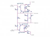
The schematic I settled on is here.
Next step was to do a layout, get some boards made, and build a couple up to try. I didn't skimp. I used quality MELF resistors, mica and poly capacitors, and a pretty good layout. One of the boards is is shown here.
Anyway, over the last couple of weeks, after a lot of delays due to doing other stuff, I finally fired one up and had a play with it.
The results are nothing short of shocking. Yes, it'll put 50W into 8 ohms, but the THD is around 0.1%. After much hair pulling, I found that the operating conditions were highly dependent on the temperature that these SOT-23 transistors were at. After much stuffing around, I found I could improve the THD to about 0.05% by putting a layer of thermally conductive goo over the whole second stage.
What a mess. Clearly these transistors need to track with one another thermally, or else all the advantages of running a balanced amplifier go totally out the window.
There's nothing that can be done to make this amplifier really useable in its current incarnation. I think I'll chalk this amp up to experience and go back to the drawing board.
A while ago, I knocked up a pair of MOSFET amps that do 140W into 8 ohms, with lovely low THD (measured 0.0013% at 1KHz). They were based on David Tilbrook's AEM6000 design, which I think is about as good a topology as you'll find for a medium-power MOSFET amp.
I was fairly conservative, and used MJE340/350 transistors for the intermediate stages, similar to Tilbrook's original.
Anyway, I knocked out a 50W (one pair of MOSFETs) version recently. Because the voltages are a little lower, I figured I could use MMBTA06/56 SOT-23 transistors for the second stage. They're faster than the MJE340/350s, and considerably smaller. All good stuff.
Simulations bore my reasoning out. With a little optimisation, I was able to go well under 0.001% THD at 1KHz, 50W into 8 ohms. All good stuff. The power dissipation of all the transistors is well within the limits for the devices.
The schematic I settled on is here.
Next step was to do a layout, get some boards made, and build a couple up to try. I didn't skimp. I used quality MELF resistors, mica and poly capacitors, and a pretty good layout. One of the boards is is shown here.
Anyway, over the last couple of weeks, after a lot of delays due to doing other stuff, I finally fired one up and had a play with it.
The results are nothing short of shocking. Yes, it'll put 50W into 8 ohms, but the THD is around 0.1%. After much hair pulling, I found that the operating conditions were highly dependent on the temperature that these SOT-23 transistors were at. After much stuffing around, I found I could improve the THD to about 0.05% by putting a layer of thermally conductive goo over the whole second stage.
What a mess. Clearly these transistors need to track with one another thermally, or else all the advantages of running a balanced amplifier go totally out the window.
There's nothing that can be done to make this amplifier really useable in its current incarnation. I think I'll chalk this amp up to experience and go back to the drawing board.
Simulations Don't Agree With Measurements
Several things you might try.
Does your simulator allow you to set different devices at differing temperatures? That may give you some insight into whether the simulations just happened to assume too optimistic PVT conditions. I would also recommend playing with the simulator to see if you can replicate the sensitivity you are seeing in the actual circuit. If you can, then it becomes much easier to examine and test possible mitigation strategies.
A couple of specifics come to mind:
In simulation, check the idle current quiescent points for the VAS and driver stages to make sure that at high voltage swings none of the devices is not near cutoff. In the actual circuit this can be accomplished by varying the idle current.
Consider modifying the VAS stage to a cascode topology. I have found that the VAS stage to be a sensitive part of the amplifier because it must support large voltage swings. A cascode topology will linearize the VAS devices quite nicely.
I am designing an amplifier of a similar topology and found that cascoding the VAS stage yielded >20 dB distortion reduction. You might want to consider that as an option.
Good luck.
suzyj said:Clearly these transistors need to track with one another thermally, or else all the advantages of running a balanced amplifier go totally out the window.
I don't intend to sound like a smart-*** but isn't it fairly obvious that a design that relies on using differentials as heavily as your circuit will also need a good balancing for their currents: The VAS might benefit from current mirrors (although they might decrease the ability to swing toward rails). In this kind of design thermal coupling of the differential transistors is understandably very important aspect as well. Maybe you should try to create a layout that allows thermal coupling of devices without using epoxy - that might involve getting rid of some of those SMD parts.
Looking at the suggestion above, I'd like to shar e my experiences.
I have tried the balanced differential vas with cascode both in simulation (superb results) and in practice (could not measure THD as I don't have the gear yet) on a circuit. If you cascode the differential VAS, you tend to ge t latch-up in most cases with the output swinging either fully high or fully low. This problem cannot be solved with an auto offset control via the input diff amps because the problem is actually in the vas stage and the diff amp(s) cannot influence it - it requires a balancing cct around each differential vas stage. I have not worked that out yet, but looking at Stochino's design, I have a feeling some of the 'glue' transistors he used around his vas are doing this. His topology is different to yours, but the cascode problem is the same. You get the same issue by the way if you use a current mirror load on th e front end diff amp in a balanced (but not differential) topology. Glen Kleinschmidt looked at this one on a post a few months ago, but there is no easy solution.
For your immediate problem, I'd suggest you go for matched integrated devices to improve the situation. For very tight matching you can use the high performance integrated matched npn and matched pnp SO8 pairs (e.g. modern equivalent of MAT01 types) or you might want to try the dual npn and pnp pairs from say NXP. These however are just small signal transistors assembled in the same package - they are not tightly matched but will be off the same wafer and closely located during the assembly process.
The holy grail for the fully balanced topology guys is to have a fully balanced front loaded with current mirrors driving a balanced, cascoded differential VAS. Key to acheiving this is to have the VAS auto balancing when the input signal is 0. I'm working on it!
Hi suzyj,
I've tried to design an amp using also a bit of the topology of the AEM6000. But I've used one stage less with even more gain than the AEM6000 (if I rememer correctly). I'm also a fan of using symmetrical diff stages.
I put directly a cascoded diff VAS in the design.
http://www.diyaudio.com/forums/attachment.php?s=&postid=801370&stamp=1135855644
http://www.diyaudio.com/forums/showthread.php?s=&threadid=70431&perpage=10&pagenumber=1
Greetz
Ben
Do you really need that many stages?, why not hook up a input stage with irf9610/610 (or better or course, but you get the general ide)..
Hmm well I got myself a thd instrument recently and I'm happy with the results I got from my amplifier, it was almost the same as in the sim in the simple simulator mode, it can do way more advanced simulations like temperature, worst case and so on..
Otherwise it's similar to the one I'm doing in topology but I'm going with inputstage:irf610/9610, output: irfp240/9140, vas: bd140,139 or similar.. It's not very expensive, I was looking at buying like buz9xx something output transistors, or like the ones you have but I couldnt really get myself to spend that much money on them.. (at least I couldnt find any cheap ones)
ben,
did you build your circuit and try it out? My VAS was very similar (all bipolar though) and I got the imbalance problem. If you take th e cascode out, the problem is reduced or removed. With single ended differential VAS there is no problem but with a fully balanced design it latches up. You will not see this on a simulation by the way.
did you build your circuit and try it out? My VAS was very similar (all bipolar though) and I got the imbalance problem. If you take th e cascode out, the problem is reduced or removed. With single ended differential VAS there is no problem but with a fully balanced design it latches up. You will not see this on a simulation by the way.
Hi,
have you looked at the voltage drop across the collector load resistors (Vr6 & Vr7=45V @ 2.5mA).
Add on the base voltage of the cascode pair and you need at least 59Vdc on the supply to run the cascodes at a tiny Vce=2.6V
Is that what you intended?
I suspect the front is not working and that's where it starts going wrong.
As an aside,
will the Zener on the cascode bases create noise? Will this noise leak into the current getting sent to the second stage?
C4 & C5 should connect to the power ground, not the clean ground.
What stabilises the output offset?
AndrewT said:Hi,
have you looked at the voltage drop across the collector load resistors (Vr6 & Vr7=45V @ 2.5mA).
Add on the base voltage of the cascode pair and you need at least 59Vdc on the supply to run the cascodes at a tiny Vce=2.6V
Is that what you intended?
I suspect the front is not working and that's where it starts going wrong.
Andrew,
There is nothing wrong with the circuit in this respect - it drops only about 15V across each of R6 and R7.
Cheers
Alex
AndrewT said:What am I misunderstanding?
That most of the current from Q7, Q8 CCS (~5mA) goes through Q5, Q6 CCS (~3.3mA) and only about 1.7 mA shared between R6 and R7
0.85mA x 18K = 15.3V
Cheers
Alex
You've forgotten Q5, which sources 3.4mA into Q7 (via the zener). The balance goes via the diff pair (800uA each side). This results in 14V across R6 & R7.
The topology is a good one. I've built a really good amp already using this topology (see http://www.littlefishbicycles.com/poweramp/). It appears to be simply the complete lack of thermal tracking in the intermediate stages that's biting me.
The topology is a good one. I've built a really good amp already using this topology (see http://www.littlefishbicycles.com/poweramp/). It appears to be simply the complete lack of thermal tracking in the intermediate stages that's biting me.
working with what you have in hand I would make a few tweaks on the board before just changing devices
loose the gnd between R17,18 if anything needs to track its the refs for these ccs
add trim pot to R19 or 20 to be able to balance mje tail curents so that the Q11-14 pairs are operating a precise balance themselves, less important but possibly trimming the MJE degeneration R could also prevent this stage' imbalnace from forcing the previous Q11-14 from operating with a noticable inbalance
you could cut your board traces and add series collector R to Q11-14 to operate the Qs at the minimum power sensitivity bias point (dropping equal V in Q Vce and total collector R)
jcx said:
you could cut your board traces and add series collector R to Q11-14 to operate the Qs at the minimum power sensitivity bias point (dropping equal V in Q Vce and total collector R)
I'd go along with this suggestion, perhaps with the addition of 100pF C's in //, not to alter the HF behavior.
Another aspect that might contribute to the problem is the "non-perfect" differential driver stage: the degeneration resistors with the tail resistor form a T attenuator that might prevent these stages from differentially cancelling the distorsion from the previous stage.
I'd also think of using "creatively" the collector currents from Q15 and 17, instead of simply dumping them to the GND. I've no precise idea yet, but I think it's worth some moments of reflection.
Cheers
LV
VAS Distortion
In taking another look at the fully differential VAS, I think I know what is happening. In order to operate correctly a 4-transistor VAS needs to maintain each VAS device in its linear region. Any deviation from that point will result in distortion. This means that the voltages presented by the second differential stage must be exactly matched to the Vbe characteristics of the four VAS devices. This is not easily achieved.
I would consider a more conventional VAS stage consisting of a pair of cascoded devices as illustrated in the attachment. Setting the idle current in this topology is substantially easier. The use of a voltage reference between the devices in the cascoded pair guarantees a fixed bias voltage within the pair. The only critical setting in this topology is to ensure that quiescent Vbe across Q13 and Q17 is set to approx 600 mV. During operation you should see less than 1 mVPP voltage swing across these points.
I have found this topology relatively insensitive to device selection and/or PVT variations.
Attachments
Re: VAS Distortion
Here's a topology modification I think Suzy's amp would lend itself to nicely:
Add another identical power output stage, driven from the collectors of Q15 and Q17. Add a opamp based DC servo to steer the common mode output voltage and apply differential feedback. Bingo - A truly symmetrical amplifier with a bridged output, differential inputs, less THD due to more complete even order harmonic cancellation and double the slew rate.
Even the 100W version, with 2 pairs of output MOSFETs would benefit from being built this way, as each pair of MOSFETs could be driven from opposite legs of the differential VAS, further improving HF performance due to the fact that the MOSFET input capacitance is now shared between both legs of the VAS.
Or just go the whole hog and do what I did (Which is esentially a AEM6000 on steroids, but without the JFET input stage):
http://users.picknowl.com.au/~glenk/MAIN.HTM
Cheers,
Glen
Elvee said:I'd also think of using "creatively" the collector currents from Q15 and 17, instead of simply dumping them to the GND. I've no precise idea yet, but I think it's worth some moments of reflection.
Cheers
LV
Here's a topology modification I think Suzy's amp would lend itself to nicely:
Add another identical power output stage, driven from the collectors of Q15 and Q17. Add a opamp based DC servo to steer the common mode output voltage and apply differential feedback. Bingo - A truly symmetrical amplifier with a bridged output, differential inputs, less THD due to more complete even order harmonic cancellation and double the slew rate.
Even the 100W version, with 2 pairs of output MOSFETs would benefit from being built this way, as each pair of MOSFETs could be driven from opposite legs of the differential VAS, further improving HF performance due to the fact that the MOSFET input capacitance is now shared between both legs of the VAS.
analog_guy said:In taking another look at the fully differential VAS, I think I know what is happening. In order to operate correctly a 4-transistor VAS needs to maintain each VAS device in its linear region. Any deviation from that point will result in distortion. This means that the voltages presented by the second differential stage must be exactly matched to the Vbe characteristics of the four VAS devices. This is not easily achieved.
I would consider a more conventional VAS stage consisting of a pair of cascoded devices as illustrated in the attachment. Setting the idle current in this topology is substantially easier. The use of a voltage reference between the devices in the cascoded pair guarantees a fixed bias voltage within the pair. The only critical setting in this topology is to ensure that quiescent Vbe across Q13 and Q17 is set to approx 600 mV. During operation you should see less than 1 mVPP voltage swing across these points.
I have found this topology relatively insensitive to device selection and/or PVT variations.
Or just go the whole hog and do what I did (Which is esentially a AEM6000 on steroids, but without the JFET input stage):
http://users.picknowl.com.au/~glenk/MAIN.HTM
Cheers,
Glen
suzyj said:Here's a really good example of "the simulations don't tell you everything".
A while ago, I knocked up a pair of MOSFET amps that do 140W into 8 ohms, with lovely low THD (measured 0.0013% at 1KHz). They were based on David Tilbrook's AEM6000 design, which I think is about as good a topology as you'll find for a medium-power MOSFET amp.
I was fairly conservative, and used MJE340/350 transistors for the intermediate stages, similar to Tilbrook's original.
Anyway, I knocked out a 50W (one pair of MOSFETs) version recently. Because the voltages are a little lower, I figured I could use MMBTA06/56 SOT-23 transistors for the second stage. They're faster than the MJE340/350s, and considerably smaller. All good stuff.
Simulations bore my reasoning out. With a little optimisation, I was able to go well under 0.001% THD at 1KHz, 50W into 8 ohms. All good stuff. The power dissipation of all the transistors is well within the limits for the devices.
The schematic I settled on is here.
Next step was to do a layout, get some boards made, and build a couple up to try. I didn't skimp. I used quality MELF resistors, mica and poly capacitors, and a pretty good layout. One of the boards is is shown here.
Anyway, over the last couple of weeks, after a lot of delays due to doing other stuff, I finally fired one up and had a play with it.
The results are nothing short of shocking. Yes, it'll put 50W into 8 ohms, but the THD is around 0.1%. After much hair pulling, I found that the operating conditions were highly dependent on the temperature that these SOT-23 transistors were at. After much stuffing around, I found I could improve the THD to about 0.05% by putting a layer of thermally conductive goo over the whole second stage.
What a mess. Clearly these transistors need to track with one another thermally, or else all the advantages of running a balanced amplifier go totally out the window.
There's nothing that can be done to make this amplifier really useable in its current incarnation. I think I'll chalk this amp up to experience and go back to the drawing board.
From what I understand of what you say here it seems to be a logical conclusion that if you used the same devices (MJE340/350) as in your other amp, the distortion should be low/similar? And this would be because they have more thermal capacity and therefore are not thermally modulated by the operating point?
Just want to make sure that I'm following.
Have you considered an effective way to thermally couple and or heat sink the smaller devices. By this I mean something better than a layer of thermal goo?
Did you match devices by the way? I do notice that you use a good amount of emitter degeneration which should reduce the need, still?
I wonder if you might have gotten some counterfeit parts that are just way off?
Nice work, by the way!
Pete B.
Suzy
Off the top of my head, changing R33 and R34 to CCS might be
worth trying.
Since they (CCS) should track each other well, an arrangement
not unlike glens IP stage with mirrors would be the way to go.
On your CCT, VAS operating point is very dependant on it's
common mode voltage. Using CCS will free it from this and should
lower distortion of Q15/16 and Q17/18 a lot. This will allow them
to work as true degenerated dif pairs.
On the down side, changing these R's to CCS will probably have
an impact on stability.
cheers
Terry
- Status
- This old topic is closed. If you want to reopen this topic, contact a moderator using the "Report Post" button.
- Home
- Amplifiers
- Solid State
- VAS thermal tracking and distortion