They are confirming they are not complementary.
That is why you will see a technical argument in favour of quasi complementary, where you design the quasi to perform as you want, using devices that are near enough identical.
That's what I was afraid of. Building an amp with those MJ15015/16 as complementary parts is thus not so practical and would not result in anything really linear.
We're ok here on this quasi build, even if someone opts to make use of the MJ15015 instead of the 2N3055, so the rails can be pumped up a bunch.
Perhaps the MJ2955 is a much closer match to the 2N3055. But then there is no way to raise the rails.
I really think a good reliable tester that can properly and non-destructively test for second breakdown, along with other parameter matching, is warranted, so parts can not only be matched, but also be carefully selected for their upper limits and used safely with chosen power rails. We all know there are many parts that will withstand far more than the very limited 60V Vce0 in the specs, but testing must be done to make sure.
Hi
ON semi (Motorola) used to put the 2N3055 with the MJ15015 on a data sheet. But the recent 2N3055/MJ2955 data sheet gives both having an fT of 2.5MHz (min).
I suspect that the older MJ15015 devices were intended to match the second breakdown performance of the old, original RCA 2N3055 (later 2N3055H). This means that they probably did use a wider base with lower fT. This is probably why some people still think the 2N3055 is "not good" for hifi.
The epi base devices which have fT's around 3Mhz are closer. BUt rather than using MJ15015/6's for higher voltages (which may be slow) I'd suggest using MJ15003/4 or going straight to the MJ21193/4 which have 4MHz fT's and linear current gain to 8A.
It is possible to design a quasi with very low crossover distortion, and I have made quite a good amp using 3055's but I would still recommend complementary pairs.
John
ON semi (Motorola) used to put the 2N3055 with the MJ15015 on a data sheet.
They still do. Just in case I went back to get their latest. They changed a few details, the 2N3055A is now 2N3055AG, but they kept the old Ft as min 0.8MHz and max 6MHz for both the 3055 and 15015, and then the 15016 still very different at min 2.2MHz and max 18MHz.
I wonder where the mistake is. Would they really make them so different (I mean the 15015 and 15016).?????
But the recent 2N3055/MJ2955 data sheet gives both having an fT of 2.5MHz (min).
Quite true. And this is confusing and makes me think there is some mistake somewhere. Why 0.8 to 6 on one sheet and min 2.5 on an other, for the same 2N3055 part??? Which is correct?
I suspect that the older MJ15015 devices were intended to match the second breakdown performance of the old, original RCA 2N3055 (later 2N3055H). This means that they probably did use a wider base with lower fT. This is probably why some people still think the 2N3055 is "not good" for hifi.
But the breakdown on the MJs is at 120V isn't it? The 3055H back then was meant for 100V.
Anyway, I think the recent 3055s should be just fine for hifi, as they would now have a higher Ft than others such as the MJ15003/4 for example, which are widely used for hifi.
The epi base devices which have fT's around 3Mhz are closer. BUt rather than using MJ15015/6's for higher voltages (which may be slow) I'd suggest using MJ15003/4 or going straight to the MJ21193/4 which have 4MHz fT's and linear current gain to 8A.
This could be done for sure. It would no longer be a 3055 based amp, but there is nothing wrong with that. After all we're trying to squeeze all we can out of the old parts, and this can still apply to the newer ones.
This would allow going much higher on the rails. Might require a few recalculations though. The protections would surely need to be recalculated for the higher soa.
It is possible to design a quasi with very low crossover distortion, and I have made quite a good amp using 3055's but I would still recommend complementary pairs.
Can you share your 3055 amp schematic? This might be interesting.
All in good fun!
")
Now that I think of it, is there any way to measure the Ft???
Could that be built into a tester that's not too complex?
After all the manufacturers must have some way to test this. They would not just specify this in datasheets only from their calculations, they would do real tests.
Could that be built into a tester that's not too complex?
After all the manufacturers must have some way to test this. They would not just specify this in datasheets only from their calculations, they would do real tests.
Last edited:
You raise several issues.
(1) Ft is not too difficult to measure. Set up a class A bias circuit at the current you want to measure the fT at. Use a low impedance collector (non-inductive) load. Make or obtain an oscillator and if necessary build a high frequency, high current drive amplifier and feed the signal into the base using a resistor, or modulate the base current using a transistor bias circuit. Measure the change in base current and the change in collector current (i.e. ac. voltage across the current monitor resistor) to obtain the gain. If you make a spot measurement at say 1 MHz then the fT will be the ratio of the two directly. If you want to check that you are in the roll-off region measure the gain at several frequencies from 100kHz to 5 MHz.
(2) I agree that if we have to use higher voltage transistors we're not talking about 3055 amps any more. But the 3055 will work from 35 V rails and as mentioned most 3055's from ST or ON Semi will be happy up to 40V - always check your devices first though.
You could of course bridge two low voltage amps - say using a couple of pairs in parallel to get 100W into 8 ohms. Actually using a fully diff amp seems to improve second harmonic by common moding.
(3) Motorola tried for years to match the second breakdown of the RCA 2N3055(H). Their MJ15015 etc was probably based on developing a high second breakdown variant. ON Semi offer the 2N3055A which is supposed to match the 2N3055H and is probably built from the same line that makes the MJ15015. I suspect that the 2N3055 is from a different line but both devices will (I suspect) be built in the same lines as other transistors with 100V or more breakdown.
So the low frequency 2N3055A is probably from one line the 2N3055 from another.
(4) There are always differences between PNP and NPN transistors that make it impossible to obtain an exact match. But some of the modern devices seem to be very good.
(5) Nothing special about a low crossover quasi. Connect the stabilising capacitor inclusive of the output stage (Miller feedback makes things worse). I used a symmetrical configuration in terms of base resistances etc without a Baxandall diode. With the output stage included in the stabilisation compensation loop the equalising diode has little effect.
John
(1) Ft is not too difficult to measure. Set up a class A bias circuit at the current you want to measure the fT at. Use a low impedance collector (non-inductive) load. Make or obtain an oscillator and if necessary build a high frequency, high current drive amplifier and feed the signal into the base using a resistor, or modulate the base current using a transistor bias circuit. Measure the change in base current and the change in collector current (i.e. ac. voltage across the current monitor resistor) to obtain the gain. If you make a spot measurement at say 1 MHz then the fT will be the ratio of the two directly. If you want to check that you are in the roll-off region measure the gain at several frequencies from 100kHz to 5 MHz.
Thanks, so this is going to be something to consider in making a good tester.
(2) I agree that if we have to use higher voltage transistors we're not talking about 3055 amps any more. But the 3055 will work from 35 V rails and as mentioned most 3055's from ST or ON Semi will be happy up to 40V - always check your devices first though.
That's the plan of course. And I am working on a bunch of leach amps as well and I wouldn't build any amp without testing and matching parts, including other important parts other than transistors.
You could of course bridge two low voltage amps - say using a couple of pairs in parallel to get 100W into 8 ohms. Actually using a fully diff amp seems to improve second harmonic by common moding.
What we're working on here on this thread is a grounded bridge, so we'll have a good amount of power even at +-35V.
And when all parts are tested and properly selected, higher rails can be considered.
(4) There are always differences between PNP and NPN transistors that make it impossible to obtain an exact match. But some of the modern devices seem to be very good.
With a large enough batch of parts, perhaps a good tester can allow making better selection and narrow the NPN and PNP's difference gap.
(5) Nothing special about a low crossover quasi. Connect the stabilising capacitor inclusive of the output stage (Miller feedback makes things worse). I used a symmetrical configuration in terms of base resistances etc without a Baxandall diode. With the output stage included in the stabilisation compensation loop the equalising diode has little effect.
Intriguing. Can you share schematics?
I've been reading Bob Cordell's stuff recently and he's obtaining some good results, at least by calculations, on many topo improvements rather easy to implement and with cheap parts. There are probably some ideas to look at for our current project..
Oh all right then.
Features: "Cherry/Stochino" high input bias current to prevent cut-off during transients, cascode driver to eliminate Early effect distortion, high VAS current to prevent VAS cut-off during transient. Output stage quasi - excellent matching between halves, low distortion (but probably not as low as could be achieved with full complementary).
Effectively a Cherry-Blameless quasi combo!
John
Attachments
Interesting.
Doesn't high current there increase noise a lot?
Why is there an extra zener D5 near the current source?
Bob Cordell described such an improvement, with the benefits. What I don't understand is the purpose of C9, which must be what you described as "inclusive of the output stage", instead of the miller cap. How does that miller cap make things worse?
That's ok, we know what we get when using quasi, but still, it's not that bad.
How low is the distortion?
What about TIM?
Have you actually built one for real or just ran sims?
Why not adding an extra pre-driver stage and 2 pairs of outputs?
Those have also good extra benefits, not to mention being able to drive heavier loads. Cordell also described this and it's all a plus to do so.
I am wondering about C1 and C7 though. Is the amp unstable without them?
What's the bandwidth obtained?
Features: "Cherry/Stochino" high input bias current to prevent cut-off during
Doesn't high current there increase noise a lot?
Why is there an extra zener D5 near the current source?
transients, cascode driver to eliminate Early effect distortion, high VAS current to prevent VAS cut-off during transient. Output stage quasi - excellent
Bob Cordell described such an improvement, with the benefits. What I don't understand is the purpose of C9, which must be what you described as "inclusive of the output stage", instead of the miller cap. How does that miller cap make things worse?
matching between halves, low distortion (but probably not as low as could be achieved with full complementary).
That's ok, we know what we get when using quasi, but still, it's not that bad.
How low is the distortion?
What about TIM?
Have you actually built one for real or just ran sims?
Why not adding an extra pre-driver stage and 2 pairs of outputs?
Those have also good extra benefits, not to mention being able to drive heavier loads. Cordell also described this and it's all a plus to do so.
I am wondering about C1 and C7 though. Is the amp unstable without them?
What's the bandwidth obtained?
Too many questions.
Yes I have built one and it sounds good. Distortion simulated is .007% at 20kHz. Bandwidth over 200kHz. If you use a Miller capacitor the VAS driver is slowed down at the very point you want it to speed up to minimise crossover distortion. This is the whole point! Yes it needs "sprog stopper" capacitors. Try to get hold of Cherry's "nested Differentiating Feedback" articles. This isn't but it uses Cherry's approach to stabilising inclusive miller feedback.
John
Too many questions.
Sorry about that, I'm just curious and I had never heard of that "nested Differentiating Feedback" before.
Yes I have built one and it sounds good. Distortion simulated is .007% at 20kHz. Bandwidth over 200kHz. If you use a Miller capacitor the VAS driver is slowed down at the very point you want it to speed up to minimise crossover distortion. This is the whole point! Yes it needs "sprog stopper" capacitors. Try to get hold of Cherry's "nested Differentiating Feedback" articles. This isn't but it uses Cherry's approach to stabilising inclusive miller feedback.
Ok cool, I'll dig something up.
Not bad result though. Probably too complex to attempt for the average diyer.
Hi all,
I am getting back to work on the calculations and spreadsheet for the VI limiter for this 3055 grounded bridge project. I've been sick for too long and not in shape to do any hobby work. Being overwhelmed with my regular work backlog, I couldn't work on the project, but progressively I am getting back to it.
On an other note, I had been trying for some time to come up with an amp design with a fully symmetrical topo and I applied several methods that are proven to address many of the problems found in ordinary amp topos. I attempted to apply what I could understand, from reliable sources, such as Bob Cordell, Douglas Self, Matti Otala, Marshall Leach, Jan Didden, etc, etc... As well as many on the forums, such as Ostripper, Bonsai, Biguns... Too many to list, there are so many good guys out there ;-)
What I had in mind was a dual diff amp 1st stage, on which I added current sources and current mirrors, a hefty output stage with 4 or 5 pairs in a triple arrangement with pre-drivers and drivers, but with a feature that I wanted, which is to arrange the full complementary in a way that brings all the collectors together, so as to not need any isolation on the heatsink and use one single heatsink, that possibly could be a forced cooled tunnel with a regulated fan blowing in. This can increase the efficiency of the heat evacuation, having only one thermal junction between the transistor cases and the heatsink. And this would allow making something very compact.
I was looking around for a good implementation of a vbe multiplier and nothing too advanced seemed like the way to go, as dual transistor types didn't seem to bring any improvement compared to a single one.
Aiming at a 85V rails design, for a healthy amount of power. I am only seeking 8 ohms loads, but I also want to oversize the output stage, so it would also handle 4 ohms and perhaps be bridgeable as well.
Several features that I wanted to keep in mind, are 1) not using any exotic parts, so it can be built by any diyer anywhere on the globe, 2) not using any static sensitive parts, such as fets/mosfets. only BGTs, 3) make an implementation as an all-in-one, with a single pcb with everything on it and avoid all wiring possible, keep it to a bare minimum, 4) avoid complexity to make it easily build-able by any diyer with little experience and make it super easy to adjust its bias, 5) avoid whenever possible the expensive parts, except perhaps for the ones that can't be avoided, such as the big filter caps, transformer, etc...
The principles sought were the symmetry from end to end, reasonably low global feedback with an amp that could possibly be stable in open loop, with each stage having a fairly low gain, the best possible linearity and lowest distortion attainable, a high slew rate, for a low tim and good stability. No complex class other than plain well known AB, however some advanced features are possible, if not too complex and fully explained and their calculations collected in spreadsheets, such as dc servos, inner feedback (like in the leach amp), separate psu for the input stage, etc...
One other thing that I thought is worth doing is doing away entirely with the VI limiting protection circuitry in favor of solid state mosfet switches (such as explored by our esteemed bonsai friend), used on each rail and the output. Those are fast and should be sufficient to efficiently protect the amp against any mishaps, and since one of the design goals is an oversized output stage with more than enough headroom, this should be indestructible.
An amp doesn't really need any volume adjustment, so it could be a simple box with a power switch, so all it needs is the input and output plugs and almost no wiring besides the toroidal transformer, with its soft start and the cooling fan. The output could be wired from the pcb to the plug, with the zobels and output coil off the pcb, but the input plug should be on the pcb and no wiring to it.
And one more thing that I think would benefit a large number of diyers out there who, like me, would really want to learn how to calculate everything but who aren't math wizs, would be to fully describe every aspect of each stage and choices, the reasons for making such choices and how the calculate everything, just like Bob Cordell or Douglas Self do in their excellent books (and Marshall Leach). Everything possibly collected in spreadsheets so a diyer could alter as needed, when their goals are different, to adapt the amp to their needs. (spreadsheets posted on the thread to remain available by all)
For sure there are likely many advanced features that some would propose to improve the design and reduce distortion, such as the nested feedback for example. Those are welcome, but should be fully described and their calculations brought to the level of the average diyer and of course put into a spreadsheet for full reproducibility.
Are there any amp hackers interested in making this work? (Bonsai? Ostripper? Bigun? many more...)
A new thread for this can be started and I would post an initial schematic to engage the discussions. I'm not a math wiz, so I can't handle the calculations myself and make spreadsheets without help, but I can work on a pcb layout afterwards and even draw in CAD the case with all the mechanical stuff.
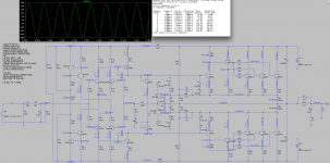
I am trying to make sense of spice with a sim of this 3055 amp. Using only the high side as we simulated before and trying to figure out the THD.
I'm attaching the sim file as it is now. I set it for a 1.3V for input signal, which gets about 28V peak to peak on the output, so roughly 50W for 8ohms load.
I see a THD of 0.03 and change... Is that about right?
How are we to interpret the FFT plot?
The protections are there but nothing really calculated, they're as they had been for some time and they don't seem to interfere with this for now.
I push the signal higher and it seems to clip at about 32V peak, so on a psu that doesn't droop too much, with the 35V on the rails, this gets close to 60W with an input at about 1.4V, but the THD goes up of course. The real thing could have its rails drop somewhat.
There is one thing I noticed though. When pushing it a little higher, such as about 1.5V input, then there is a kind of clipping towards the low rail but not the top. So it's not quite symmetric. How can we track this? Where does this difference could come from? Can this be corrected somehow?
Then I'm thinking about using this later to verify the protection action. What's the best way to test this?
Attachments
Try simulating without the protection circuit.
Yes, I thought of that and I disabled it by disconnecting the diodes. But it didn't change anything, so it can't be the protections.
Something makes it unsymmetrical.
I lowered the load to 4ohms and it just makes it more important, not that much, but enough to bring the THD up somewhat.
Ok, I put the input signal back where it belongs before the input cap. I upped that input cap's value, but that's besides the point.
I thought that by adding a source to add an offset to the signal it would cancel out most of the existing offset present on the output (about 32mV), but now that I moved the input signal to before that input cap, it's useless, so I left it but put it at 0V.
Anyway, I was surprised to see that unsymmetrical defect go away with the input source before that input cap, even more, when the output offset went down from around 32mV to some 3.8uV...
The signal on the output is better now and at 1.3V on the input, we get about 28V peak and I put the load at 8ohms. The THD is then about 0.0293 and it's a little before clipping, but basically full nominal power.
That distortion goes up a bit on the 4 ohms load, but not hugely.
However I'm thinking perhaps there are a few things to do that could make this a little better still. Any ideas?
The protection is disconnected with its diodes' legs lifted.
Attachments
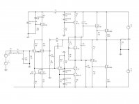
Alright, I did some tweaking on several values and here is a screenshot of what I have so far.
The offset on the output is tiny, due to the values tweaked on the diff amps.
I tried reducing the bias current because I though it was rather high, at more than 60mA per power transistor, and when I reduced this, there were still no signs of crossover distortion increase all the way down around 20mA per transistor. But to arrive at this low bias current, the trimmer (P1) value was down to 3ohms. I readjusted this to about 30mA, for a total of nearly 100mA, and that works fine, although it would work with a lower bias current.
The thing is, this brought to mind the fact that not only the bias trimmer will have to be adjusted just about all the way down, my concern is that in case the wiper loses contact, we'd get a huge increase in bias, which could be devastating.
So now I'm thinking it might be a good idea to revisit this bias spreader issue and find a better and safer way to do this. I don't trust it.
And if there is any way to make current mirrors working on the diff amps, it would make a good amount of difference. As ingenieus had suggested it before and ran a few sims. It might be worth the effort.
During my exploration with the tweaks, I reduced the overall gain via the global feedback, just a bit, but although the needed signal strength on the input would need to be greater to achieve full power, the THD went down to a tiny bit above 0.01%, which to me shows that by doing a little extra in the diff amp with the addition of current mirrors, we might reach a nice distortion level.
I played with the base stopper resistors on the outputs, and also the base resistors and degeneration ones on the diff amps. More simulation is needed to find out what all this did to other aspects, but so far the result seems to look nice.
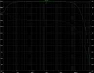
I adjusted the caps on the input and the feedback for a lower high pass frequency and tweaked the high pass as well. The ac analysis now shows a rather flat response over the whole audio range, a low frequency cut off below 2Hz and the high somewhere above 160kHz.
I know the simulations are likely to be a little generous, but it looks like the result can be rather nice anyway.
What I'd like to know, is how to simulate to find out if there are any possibilities of oscillations. Is it even possible to locate and see where there could be any?
I am even thinking we could add base stoppers on the drivers, even if small values, in case there is any chance for oscillations.
However, when ingenieus did his early sims on the early versions when we were still working on the improvements, he had mentioned a phase margin of at least 50degrees, and so there were no signs of possible instabilities.
How is this simulated, to find out where we stand now, and what would happen if the current mirrors were added to the diff inputs?
If the bias spreader is changed to something safer, how would it affect it? And perhaps we could also improve the vas at the same time, which might be required to make the current mirrors work on the diff amps.
The offset on the output is tiny, due to the values tweaked on the diff amps.
I tried reducing the bias current because I though it was rather high, at more than 60mA per power transistor, and when I reduced this, there were still no signs of crossover distortion increase all the way down around 20mA per transistor. But to arrive at this low bias current, the trimmer (P1) value was down to 3ohms. I readjusted this to about 30mA, for a total of nearly 100mA, and that works fine, although it would work with a lower bias current.
The thing is, this brought to mind the fact that not only the bias trimmer will have to be adjusted just about all the way down, my concern is that in case the wiper loses contact, we'd get a huge increase in bias, which could be devastating.
So now I'm thinking it might be a good idea to revisit this bias spreader issue and find a better and safer way to do this. I don't trust it.
And if there is any way to make current mirrors working on the diff amps, it would make a good amount of difference. As ingenieus had suggested it before and ran a few sims. It might be worth the effort.
During my exploration with the tweaks, I reduced the overall gain via the global feedback, just a bit, but although the needed signal strength on the input would need to be greater to achieve full power, the THD went down to a tiny bit above 0.01%, which to me shows that by doing a little extra in the diff amp with the addition of current mirrors, we might reach a nice distortion level.
I played with the base stopper resistors on the outputs, and also the base resistors and degeneration ones on the diff amps. More simulation is needed to find out what all this did to other aspects, but so far the result seems to look nice.
I adjusted the caps on the input and the feedback for a lower high pass frequency and tweaked the high pass as well. The ac analysis now shows a rather flat response over the whole audio range, a low frequency cut off below 2Hz and the high somewhere above 160kHz.
I know the simulations are likely to be a little generous, but it looks like the result can be rather nice anyway.
What I'd like to know, is how to simulate to find out if there are any possibilities of oscillations. Is it even possible to locate and see where there could be any?
I am even thinking we could add base stoppers on the drivers, even if small values, in case there is any chance for oscillations.
However, when ingenieus did his early sims on the early versions when we were still working on the improvements, he had mentioned a phase margin of at least 50degrees, and so there were no signs of possible instabilities.
How is this simulated, to find out where we stand now, and what would happen if the current mirrors were added to the diff inputs?
If the bias spreader is changed to something safer, how would it affect it? And perhaps we could also improve the vas at the same time, which might be required to make the current mirrors work on the diff amps.
Attachments
I have seen me get as low as 10mA per transistor in class ab amplifiers.
Peavey are a big fan of low bias currents. If its good for them then its good for me.
Why waste power into the heat sink ?
Peak do a good transistor tester. It doesn't even care how you connected it up !
Peak Electronic Design Limited - Atlas DCA - Semiconductor Analyser - Model DCA55
Peavey are a big fan of low bias currents. If its good for them then its good for me.
Why waste power into the heat sink ?
Peak do a good transistor tester. It doesn't even care how you connected it up !
Peak Electronic Design Limited - Atlas DCA - Semiconductor Analyser - Model DCA55
I have seen me get as low as 10mA per transistor in class ab amplifiers.
Peavey are a big fan of low bias currents. If its good for them then its good for me.
Why waste power into the heat sink ?
Exactly!
This amp doesn't show any signs of crossover issues with about 20mA per transistor, and it likely is still fine even lower, but it couldn't be tested that low because the bias spreader won't go that far down.
Peak do a good transistor tester. It doesn't even care how you connected it up !
Peak Electronic Design Limited - Atlas DCA - Semiconductor Analyser - Model DCA55
I looked at that one recently, and it may be ok for matching parts, but only for one single point and not a curve. What it doesn't do is test for secondary breakdown and test power transistors at high currents.
Not being any good at AC analysis, here are some thoughts.
CFP gurus are welcome to come back with corrections, or a complete re-write.
This is not a conventional EF output stage.
The pre-driver is the EF.
The CFP after that pre-driver is a current multiplier.
Look at the Vre of the pre-driver.
730uA and 68ohms = 50mVre.
It is already overbiased, cf. optimal EF bias.
- Home
- Amplifiers
- Solid State
- Amplifier based on 2N3055