"Would you have a higher resolution of that schematic sheet? "
Sorry, no.
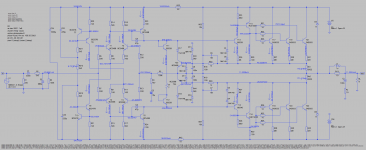
That is the only copy of the Hadley that I have come across. I used it as the basis of the complementary design I posted below it. The new one should be clear enough to show how it works. I think Bongiorno worked for Hadley about that time frame, and I know Nelson Pass was aware of it.
Oh well! It's an interesting one, because it's a bridge to begin with and it has a low number of parts. I wonder how that one would perform when there is a fault on the outputs, if the speakers would be at risk.
One also interesting feature is the fact that it's also a quasi. We could use 3055s throughout as well.
I grabbed LTSpice for mac (I'm on mac) so I could try making a simulation, with the protection added and verify various assumptions and ideas.
That mac version is crippled, not because it's done for commercial purposes, since it's free, but perhaps because the port isn't finished. It's supposed to be a wine bottled version, so it's supposed to be the windows environment under which it runs anyway, so I don't understand why it's crippled that way. Anyway I must use manual editing and other tricks to get things to work.
I'm a total beginner at spice, so I surely can't master all its intricacies and get the best and proper sims done. I'm doing what I can with the schematic capture and when I think it may be somewhat functional, I will post that spice file. I will include all the models in the file itself so it should work out of the box when someone else opens it.
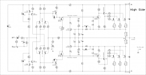
I usually choose R18 and R62 such that R65 is unnecessary, but it's not the only way to do this. The drop is R22 and R45 is inconsequential to the protection circuits
The use of R65/87 is to do VI limiting instead of just I. So if you ommit R65/87, then it's only an I limiter.
From the spice sim that I'm trying to assemble (almost done), I can see the drop in R22/45 is around 1.5V, more or less. Perhaps it wouldn't change much how the V limiting works, but it also may somewhat, when we're not in a short situation but just a low load and the output does swing close to the rails, then how can the V limiting work properly if we're so close to the drop in emmiter resistors plus the Vce in the outputs, which is close to Vcesat in such cases...
I will be posting shortly an output of that spice sim with the operating point info on it. We'll see about other analysis later.
What I get so far doesn't make sense to me, because I am getting offsets even when I hook the input to gnd, and I did that right on the base resistors on the input diff to make sure. With that one at 0V, the other side logically should also be there.
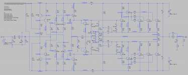
So here it is.
Don't pay attention to the values in the protection circuit, I put the parts there and used values that won't trigger it when at operating point.
I tried playing with several values of P1 (should be a pot there, but I just choose the resistor's value) and it looks like this small value should be lowering the bias more than that. I was at 20ohms a bit earlier and the bias was over 190mA per output.
The part that doesn't make sense to me is that having the input at gnd (base res R6&7) should get rid of whatever offset and everything should be 100% balanced. So what's causing this out of balance situation? We're not dealing with variation between parts, so what is it then? Bad models?
Attachments
It's R43 and 44 which turn it into a VI limiter. They allow the current to go above Isc when VCE decreases. R65 causes the lagging inductive current to be limited to values less than the short circuit current. Since these excursions are of such short duration and mostly non-repetitive, I've found limiting to less than Isc to be unnecessary. Of course, to be completely general about the limiting circuitry, leave it in.
You have about 4mV of offset attributable to differential balance. You could trim that out if you wanted to, it's on the order of a run of the mill opamp and nothing to worry about. You have another 37mV caused by input offset and bias currents. The feedback resistors are a bit too large for a bipolar input stage. Divide the feedback resistors and input bias resistors by 10, and then all sources of offset will be on the same order of magnitude. At that point, it will require careful component matching or LTP load resistor trimming to get it any better.
It's R43 and 44 which turn it into a VI limiter. They allow the current to go above Isc when VCE decreases. R65 causes the lagging inductive current to be limited to values less than the short circuit current. Since these excursions are of such short duration and mostly non-repetitive, I've found limiting to less than Isc to be unnecessary. Of course, to be completely general about the limiting circuitry, leave it in.
But those need to be calculated properly, so we have a bunch of calculations to do now. I arbitrarily chose values and corrected them to prevent the action with no signal. I will remove that gnd connection to allow sims to be done now with a signal.
You have about 4mV of offset attributable to differential balance.
It seems odd that there could be such an offset, on a completely complementary design (except the outputs), with just about everything symetric, especially on the diff stage and we're not dealing with the real world parts differences.
The feedback resistors are a bit too large for a bipolar input stage. Divide the feedback resistors and input bias resistors by 10, and then all sources of offset will be on the same order of magnitude. At that point, it will require careful component matching or LTP load resistor trimming to get it any better.
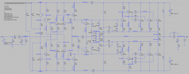
It's true this does reduce that offset. I took out the gnd shunt from the input and the offset on the amp output when down from around 40mV to about 11mV. Then I dropped the value of R5 from 100k to 10k, R4 from 4k7 to 470 and R3 to 10k as well, and the offset is down further (see new sim attached).
If this pushes to match the input diffs even more precisely, then it may not be a good idea. Although I am planning on matching as much as possible all the parts (including resistors and caps...). doing it very precisely may not be practical enough.
One thing is still puzzling, is the bias current in the outputs being so high even with that P1 down to 10ohms only.
Attachments
you have complementary PNP & NPN pairs on the input.
If the models have different hFE then you will get output offset due to differing base currents.
If the Vbe between the N & P are different this gives a second source of output offset. Again this is caused by model differences.
If the simulation is passing different currents through the four input transistors, then this is a third source of output offset.
It is relatively easy to modify the simulated amplifier to reduce these three offsets to near zero mVdc.
When you come to build the amplifier you can do the same thing to reduce the actual amplifier offset to near zero mVdc.
Or you can trim the offset with a crude pot adjustment and accept the unbalanced front end and the distortion that is likely to emanate.
Here is an other sim. I am posting the spice file too. I included the models not included with LTSpice in the asc file so it would run out of the box. Let me know if it doesn't.
I reverted the feedback values to the original ones, although that does improve the offset slightly, it also changes the high pass frequency on the input and we were getting close to 100hz instead of somewhere near 10hz...
I lowered P1 to 5 ohms and the bias seems still rather high.
The protection circuit is not active, with around 300mV on the tr bases.
I changed the pre-drivers to the BC639/640 instead of the BC546/556, since those would be too weak to handle this and probably too close for comfort on their Vce0 anyway.
What's wrong with the bias? It's too high, even with P1 adjusted so low...
Attachments
If the models have different hFE then you will get output offset due to differing base currents.
If the Vbe between the N & P are different this gives a second source of output offset. Again this is caused by model differences.
I figured it had something to do with the models, but I suppose it kind of makes it like the real world with slight differences. And this doesn't mean those models are bad then.
It is relatively easy to modify the simulated amplifier to reduce these three offsets to near zero mVdc.
When you come to build the amplifier you can do the same thing to reduce the actual amplifier offset to near zero mVdc.
Or you can trim the offset with a crude pot adjustment and accept the unbalanced front end and the distortion that is likely to emanate.
I think it's too small to worry about and the real build will be different from the sim anyway.
And I do plan to do as much matching as possible, even if not perfect, this should help.
I'm not trying to dig deeper in the simulation. And I would like to know why the bias won't come down enough.
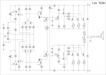
Look at the front end.
The four transistors are all running at different currents.
If you want the sim to give you zero offset as a result of balancing the front end transistors, then YOU must make adjustments to get those currents identical.
First: adjust R20 to get the tail current up from 588.276uA to 600.022uA to match the upper half. Does that change the output offset?
Second: adjust R15 so that Ir9 exactly equals Ir11. Then change R17 to match (keeps the Vce the same for both devices. Due to Early Effect you make need to readjust R15.
Does that change the output offset?
Third: adjust R14 as previous paragraph. Does that change the offset?
Fourth: etc ......
What you do in the simulation to bring the front end into balance is the same as you SHOULD be doing to the real amplifier if precision is your goal. The values WILL BE DIFFERENT, the process will be the same.I figured it had something to do with the models, but I suppose it kind of makes it like the real world with slight differences. And this doesn't mean those models are bad then.
I think it's too small to worry about and the real build will be different from the sim anyway.
And I do plan to do as much matching as possible, even if not perfect, this should help.
I'm not trying to dig deeper in the simulation. And I would like to know why the bias won't come down enough.
You will need to use larger area transistors in the bias stack. The bigger predrivers now have a lower Vbe for a given base current. You don't need a high fT device in the bias stack - don't be afraid to use something beefy.
10 or 20 mV of offset is no big deal. A few % out of balance in the front end may be the dominant source of THD at 100 Hz, but it sure won't be at 10k with 4 ohm load. You won't get any .000007% out of this anyway. I wouldn't sweat it beyond a reasonable attempt at matching the diff pairs.
10 or 20 mV of offset is no big deal. A few % out of balance in the front end may be the dominant source of THD at 100 Hz, but it sure won't be at 10k with 4 ohm load. You won't get any .000007% out of this anyway. I wouldn't sweat it beyond a reasonable attempt at matching the diff pairs.
You will need to use larger area transistors in the bias stack. The bigger predrivers now have a lower Vbe for a given base current. You don't need a high fT device in the bias stack - don't be afraid to use something beefy.
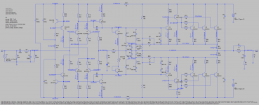
Ok, this is a good thing I'm checking on this now, otherwise there would've been issues in a real build. Even with P1 shorted, the bias current would probably have stay a little high.
I put the same BC639 as the pre-drivers, and since they are meant to be facing each other and thermally coupled, they should remain as TO92s.
This is working much better now, although the adjustment of P1 seems still rather low, but with 7ohms we got around 55mA per output. Not too bad. It's good that I'm catching this, before making pcbs, since that TO92 I think doesn't have the same pinout as the others, that will change routing.
A few % out of balance in the front end may be the dominant source of THD at 100 Hz, but it sure won't be at 10k with 4 ohm load. You won't get any .000007% out of this anyway. I wouldn't sweat it beyond a reasonable attempt at matching the diff pairs.
That's what I was aiming for. And it seems we may yet get better than 0.1%, which really isn't that bad, considering what we're using.
Attachments

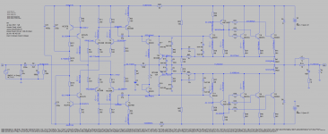
Have you looked at the >2:1 ratio of current in the two drivers Q15/16 ?
Put R38, 40, 42 in the emitters not the collectors - that will probably better balance the drive Ic's.
Where is my post from more than 30minutes ago?
Apparently they're showing later, I see them now. I will look into this now in the sims.
Have you looked at the >2:1 ratio of current in the two drivers Q15/16?
I didn't before, with all this imbalance, I didn't notice something specific, but now that you mention it, YES!!! This looks odd.
SO! I tried something (see sims attached).
Oddly enough, bringing down R28 to the - Rail catches up on some of that difference, and I don't understand why (not surprising) but it also lowers those idling currents in those drivers.
What to make of it? I had first done that in the early versions and then later brought R28 back up as it was in the original schematic. It causes the error to be lower, but one additional imbalance to compensate for another isn't good anyway. So what could be causing that imbalance? I don't think R28 should stay that way.
Attachments
- Home
- Amplifiers
- Solid State
- Amplifier based on 2N3055