Re: Bipolar - MOS crossover issues
Hi Rodolfo,
It's a good idea, but where do we get the right models? Most of us (not me) are using level 3 models, which are useless for this purpose, as they do not take into account the weak inversion. Therefore, simulating the cross-over spectra makes only sense when using BSIM3.3 (level 8) or higher models
To all,
For the same reason, ignore what D. Self has to say about MOSFET output stages, as most of his "insight" is based on flawed simulations.
Cheers, Edmond.
ingrast said:[snip]
Probably this single issue - crossover distortion - merits a similar treatment for MOS output stages, and probably this thread is more appropiate for it, so here is the proposal.
- Simulate similar power level MOS output stages and analyze crossover spectral structure and variation with operating conditions (bias level etc.)
[snip]
Rodolfo
Hi Rodolfo,
It's a good idea, but where do we get the right models? Most of us (not me) are using level 3 models, which are useless for this purpose, as they do not take into account the weak inversion. Therefore, simulating the cross-over spectra makes only sense when using BSIM3.3 (level 8) or higher models
To all,
For the same reason, ignore what D. Self has to say about MOSFET output stages, as most of his "insight" is based on flawed simulations.
Cheers, Edmond.
Re: Re: Bipolar - MOS crossover issues
That's the point, my feeling is there is progress to be made beyond the unavoidably simplifying assumptions made with analytical models (pencil and paper, closed form) and the first generation Spice models. Andy_c has been working on this and certainly others too.
Rodolfo
estuart said:
.... but where do we get the right models? Most of us (not me) are using level 3 models, which are useless for this purpose, as they do not take into account the weak inversion. Therefore, simulating the cross-over spectra makes only sense when using BSIM3.3 (level 8) or higher models......
That's the point, my feeling is there is progress to be made beyond the unavoidably simplifying assumptions made with analytical models (pencil and paper, closed form) and the first generation Spice models. Andy_c has been working on this and certainly others too.
Rodolfo
Re: Re: Re: Bipolar - MOS crossover issues
Hi Rodolfo,
I have given my home brew level 8 models of 2SJ201/2SK1530 to Andy. Perhaps he is willing to do such analysis. Me myself haven't enough time at the moment, I'm too busy with a sub ppm amp (with output coils made from YBa2Cu3O7 ).
).
Cheers, Edmond.
ingrast said:That's the point, my feeling is there is progress to be made beyond the unavoidably simplifying assumptions made with analytical models (pencil and paper, closed form) and the first generation Spice models. Andy_c has been working on this and certainly others too.
Rodolfo
Hi Rodolfo,
I have given my home brew level 8 models of 2SJ201/2SK1530 to Andy. Perhaps he is willing to do such analysis. Me myself haven't enough time at the moment, I'm too busy with a sub ppm amp (with output coils made from YBa2Cu3O7
).Cheers, Edmond.
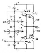
anatech said:If Sansui engineers wrote a patent application, they are attempting to "own it". Either that or no one searches for prior art on either end in hopes of getting away with it.
Chris,
Sansui wrote an AES paper, not a patent application. They were essentially putting their idea into the public domain. So in that sense, it was OK for Levinson to use it. But the disgusting part is that Levinson claimed that THEY developed it. Here is the Sansui circuit:
Attachments
Re: Re: Re: Re: Bipolar - MOS crossover issues
Hope yu are chilling them with liquid helium in Bose - Einsten condensate form ...
Rodolfo
estuart said:
....sub ppm amp (with output coils made from YBa2Cu3O7
Cheers, Edmond.
Hope yu are chilling them with liquid helium in Bose - Einsten condensate form ...
Rodolfo
Re: Re: Bipolar - MOS crossover issues
I don't know that Self's work is SO flawed that it should be IGNORED.
Perhaps the models aren't EXACTLY correct. But if you have read his book and looked at the graphs of the output stage of gain versus signal swing, it is OBVIOUS that there is no way to get an overlap (which is essentially what the bias does) such that the sum of the two transfer curves is even CLOSE to flat.
You don't need a super-fancy model to tell you that -- FET's are essentially square-law devices....
estuart said:For the same reason, ignore what D. Self has to say about MOSFET output stages, as most of his "insight" is based on flawed simulations.
I don't know that Self's work is SO flawed that it should be IGNORED.
Perhaps the models aren't EXACTLY correct. But if you have read his book and looked at the graphs of the output stage of gain versus signal swing, it is OBVIOUS that there is no way to get an overlap (which is essentially what the bias does) such that the sum of the two transfer curves is even CLOSE to flat.
You don't need a super-fancy model to tell you that -- FET's are essentially square-law devices....
Re: Re: Re: Re: Bipolar - MOS crossover issues
If you mix in some U238 you will have more brilliance
Jan Didden
estuart said:[snip]I'm too busy with a sub ppm amp (with output coils made from YBa2Cu3O7
Cheers, Edmond.
If you mix in some U238 you will have more brilliance
Jan Didden
Re: Re: Re: Re: Re: Bipolar - MOS crossover issues
Hi Rodolfo and Jan,
Thank you for the good advice! And Jan, very kind of you to not recommend U235, despite it gives even more brilliance.
Cheers, Edmond.
ingrast said:Hope yu are chilling them with liquid helium in Bose - Einsten condensate form ...
Rodolfo
janneman said:If you mix in some U238 you will have more brilliance
Jan Didden
Hi Rodolfo and Jan,
Thank you for the good advice!
And Jan, very kind of you to not recommend U235, despite it gives even more brilliance.Cheers, Edmond.
Re: Re: Re: Bipolar - MOS crossover issues
But they're only square law devices above the threshold voltage. Below the threshold voltage, the drain current is an exponential function of Vgs, similar to a BJT. For more info on this, see this PowerPoint presentation from a Ga. Tech course, especially slide 10. Note the current scale of slide 10 is logarithmic.
This may seem like a trivial point, but Self is using derivatives to magnify small variations in the slope of the nonlinear input-output characteristic. As was shown earlier in this thread, the second derivative of Id vs. Vgs for the old square law curve is discontinuous at the threshold voltage. It's zero below threshold, and jumps to a non-zero constant above threshold. This discontinuity will give rise to sudden changes in the slope of Vout vs. Vin in the simulation that don't correctly represent real life behavior.
I'll try to post some plots similar to Self's for FET output stages later today. I have Edmond's BSIM3 models for the 2SJ201 and 2SK1530. I'll put these on the same plot as some IRFP244 and FQA12P20 models that use SPICE level 1.
Charles Hansen said:You don't need a super-fancy model to tell you that -- FET's are essentially square-law devices....
But they're only square law devices above the threshold voltage. Below the threshold voltage, the drain current is an exponential function of Vgs, similar to a BJT. For more info on this, see this PowerPoint presentation from a Ga. Tech course, especially slide 10. Note the current scale of slide 10 is logarithmic.
This may seem like a trivial point, but Self is using derivatives to magnify small variations in the slope of the nonlinear input-output characteristic. As was shown earlier in this thread, the second derivative of Id vs. Vgs for the old square law curve is discontinuous at the threshold voltage. It's zero below threshold, and jumps to a non-zero constant above threshold. This discontinuity will give rise to sudden changes in the slope of Vout vs. Vin in the simulation that don't correctly represent real life behavior.
I'll try to post some plots similar to Self's for FET output stages later today. I have Edmond's BSIM3 models for the 2SJ201 and 2SK1530. I'll put these on the same plot as some IRFP244 and FQA12P20 models that use SPICE level 1.
Re: Re: Re: Bipolar - MOS crossover issues
Hi Charles,
I've read Self's book and agree with much of what he has said about crossover distortion. It's a complex subject, and even he could have gone much further, both in his treatment of BJT and MOSFET crossover distortion. But of course there is always a practical limit to how much space can be devoted to one subject.
It is certainly true that there is no "optimum" Class-AB bias point for MOSFET crossover distortion, and it can be more difficult to deal with than with BJTs largely because of the transconductance being about 10X lower at a given operating current for the MOSFETs. This inevitable transconductance droop in the crossover region of a Class-AB MOSFET output stage is the main reason I applied Hawksford error correction to my original MOSFET power amplifier. Even then, I was still biasing it at about 150 mA.
Very good MOSFET power amps can of course be made without resort to error correction. To a certain extent, the simple answer is that you need higher idle bias in a MOSFET design to get competitive with the BJT crossover THD numbers. That ends up giving you a bigger Class-A region at the same time. Indeed, if you built a big amp like the JC-1 with nine MOSFET pairs each idling at about 150 mA, you would have a pretty low-distortion output stage.
I think that the study of MOSFET output stage crossover distortion using SPICE, as was done for the BJTs, would be very worthwhile if we had models we could trust insofar as the crossover distortion aspects were concerned. The fact that the MOSFET characteristic is somewhat more gradual than the rather abrupt BJT characteristic might make a difference in the nature of the crossover distortion that we see (such as what harmonics are predominant).
Cheers,
Bob
Charles Hansen said:
I don't know that Self's work is SO flawed that it should be IGNORED.
Perhaps the models aren't EXACTLY correct. But if you have read his book and looked at the graphs of the output stage of gain versus signal swing, it is OBVIOUS that there is no way to get an overlap (which is essentially what the bias does) such that the sum of the two transfer curves is even CLOSE to flat.
You don't need a super-fancy model to tell you that -- FET's are essentially square-law devices....
Hi Charles,
I've read Self's book and agree with much of what he has said about crossover distortion. It's a complex subject, and even he could have gone much further, both in his treatment of BJT and MOSFET crossover distortion. But of course there is always a practical limit to how much space can be devoted to one subject.
It is certainly true that there is no "optimum" Class-AB bias point for MOSFET crossover distortion, and it can be more difficult to deal with than with BJTs largely because of the transconductance being about 10X lower at a given operating current for the MOSFETs. This inevitable transconductance droop in the crossover region of a Class-AB MOSFET output stage is the main reason I applied Hawksford error correction to my original MOSFET power amplifier. Even then, I was still biasing it at about 150 mA.
Very good MOSFET power amps can of course be made without resort to error correction. To a certain extent, the simple answer is that you need higher idle bias in a MOSFET design to get competitive with the BJT crossover THD numbers. That ends up giving you a bigger Class-A region at the same time. Indeed, if you built a big amp like the JC-1 with nine MOSFET pairs each idling at about 150 mA, you would have a pretty low-distortion output stage.
I think that the study of MOSFET output stage crossover distortion using SPICE, as was done for the BJTs, would be very worthwhile if we had models we could trust insofar as the crossover distortion aspects were concerned. The fact that the MOSFET characteristic is somewhat more gradual than the rather abrupt BJT characteristic might make a difference in the nature of the crossover distortion that we see (such as what harmonics are predominant).
Cheers,
Bob
lumanauw said:Mr. Hansen, have you try or make a product with one from these "non-turnoff" scheme?
No, only simulations. But I got enough information from these to realize that it was a dead end. You can get MUCH better results simply by adding additional paralleled output devices...
Re: Re: Re: Re: Bipolar - MOS crossover issues
John's amps use MOSFET's for the drivers. The outputs are bipolars.
I built an amp with 32 (lateral) MOSFET's per channel. Measured darned good (especially considering zero feedback), sounded great. But stupidly expensive and also a lot of heat and power consumption.
The MOSFET's were the Semelab (Exicon) devices. They are $5 each in quantity, so that is $320 in parts cost just for the output transistors! Plus I was running them at 120 mA, which is their zero tempco point. With 33 volt rails, that is 125 watts per channel for the output stage. That is a lot of heat to get rid of and a lot of money for the power bill.
And the sound (and measurements) get better as the bias current is increased, essentially without limit. If there are no practical concerns, it is a good way to go.
But with a BJT stage I can get better sound, better measurements, lower cost, lower heat, and lower power dissipation. Kind of a no-brainer in my book....
Bob Cordell said:Indeed, if you built a big amp like the JC-1 with nine MOSFET pairs each idling at about 150 mA, you would have a pretty low-distortion output stage.
John's amps use MOSFET's for the drivers. The outputs are bipolars.
I built an amp with 32 (lateral) MOSFET's per channel. Measured darned good (especially considering zero feedback), sounded great. But stupidly expensive and also a lot of heat and power consumption.
The MOSFET's were the Semelab (Exicon) devices. They are $5 each in quantity, so that is $320 in parts cost just for the output transistors! Plus I was running them at 120 mA, which is their zero tempco point. With 33 volt rails, that is 125 watts per channel for the output stage. That is a lot of heat to get rid of and a lot of money for the power bill.
And the sound (and measurements) get better as the bias current is increased, essentially without limit. If there are no practical concerns, it is a good way to go.
But with a BJT stage I can get better sound, better measurements, lower cost, lower heat, and lower power dissipation. Kind of a no-brainer in my book....
Re: Re: Re: Bipolar - MOS crossover issues
Hi Charles,
I did not say that Self's work should be ignored. Such phrase could easily be read as all his work should be ignored. I'm a great fan of Self, I have his book and copies of (almost) all his publication in WW. I do agree with him in almost every respect, but not regarding MOSFETs (and I'm not the only one).
I do know that there isn't a perfect overlap, but that's a minor issue. Just measuring the voltage gain of a MOSFETs O/P sage gives a false impression. What really counts is the behavior when embedded in a complete amp, which of course should be optimized for MOSFETs.
As for "super-fancy models", it make a big difference whether using level 3 or level 8 models, in particular with respect to higher cross-over harmonics. Such a big difference that one is totally misled by the simple models. Maybe that designers of high distortion amps are happy with low level models, but I'm involved in sub ppm designs and need something better.
BTW, I suppose that the guys at Berkeley are not amused if you call their effort "super-fancy".
FET's, that is, vertical power MOSFETs, are not essentially square-law devices, only in a certain region. Biased as class-b or class-ab, the weak inversion plays an important role and in this region MOSFETs behave exponential.
One more thing: please don't shout at me, use italics, for example, instead of CAPITALS.
Cheers, Edmond.
Charles Hansen said:I don't know that Self's work is SO flawed that it should be IGNORED.
Perhaps the models aren't EXACTLY correct. But if you have read his book and looked at the graphs of the output stage of gain versus signal swing, it is OBVIOUS that there is no way to get an overlap (which is essentially what the bias does) such that the sum of the two transfer curves is even CLOSE to flat.
You don't need a super-fancy model to tell you that -- FET's are essentially square-law devices....
Hi Charles,
I did not say that Self's work should be ignored. Such phrase could easily be read as all his work should be ignored. I'm a great fan of Self, I have his book and copies of (almost) all his publication in WW. I do agree with him in almost every respect, but not regarding MOSFETs (and I'm not the only one).
I do know that there isn't a perfect overlap, but that's a minor issue. Just measuring the voltage gain of a MOSFETs O/P sage gives a false impression. What really counts is the behavior when embedded in a complete amp, which of course should be optimized for MOSFETs.
As for "super-fancy models", it make a big difference whether using level 3 or level 8 models, in particular with respect to higher cross-over harmonics. Such a big difference that one is totally misled by the simple models. Maybe that designers of high distortion amps are happy with low level models, but I'm involved in sub ppm designs and need something better.
BTW, I suppose that the guys at Berkeley are not amused if you call their effort "super-fancy".
FET's, that is, vertical power MOSFETs, are not essentially square-law devices, only in a certain region. Biased as class-b or class-ab, the weak inversion plays an important role and in this region MOSFETs behave exponential.
One more thing: please don't shout at me, use italics, for example, instead of CAPITALS.
Cheers, Edmond.
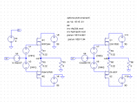
As I mentioned earlier, I wanted to do a sim that looks at the effect of modeling the weak inversion (AKA sub-threshold conduction) of MOSFETs on plots of output stage behavior like what Self did in his book. In the third edition of his book, on page 319, he takes a complementary source follower and looks at the derivative of the output voltage with respect to the input, for an input DC sweep from -15 to +15 Volts, presumably with an 8 Ohm load.
I did the same thing using the simulation whose schematic is shown below. The idea is to have two almost identical circuits, one using a MOSFET level 1 model, and the other using Edmond's BSIM3 models of the 2SJ201 and 2SK1530. Unfortunately, the only BSIM3 models I have are of these two devices, and I do not have level 1 models for them. So I instead chose the IRFP244 and FQA12P20, for which I hand fit the data from the datasheet graphs to a level 1 model. So the comparison is not perfect, as the Toshiba devices have higher transconductance, and therefore less distortion. For each circuit, I adjusted the bias voltages to get DC drain currents of 150 mA. Here is the schematic.
I did the same thing using the simulation whose schematic is shown below. The idea is to have two almost identical circuits, one using a MOSFET level 1 model, and the other using Edmond's BSIM3 models of the 2SJ201 and 2SK1530. Unfortunately, the only BSIM3 models I have are of these two devices, and I do not have level 1 models for them. So I instead chose the IRFP244 and FQA12P20, for which I hand fit the data from the datasheet graphs to a level 1 model. So the comparison is not perfect, as the Toshiba devices have higher transconductance, and therefore less distortion. For each circuit, I adjusted the bias voltages to get DC drain currents of 150 mA. Here is the schematic.
Attachments
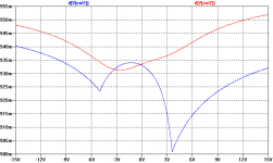
And here is the plot of the derivative of V(out) vs. V(in) for the two model types. The "kinky" one uses the level 1 model for IRFP244 and FQA12P20. The smooth one is for Edmond's BSIM3 models.
I think it's pretty clear that the level 1 models are completely wrong. The "kinks" in the curve result from the discontinuity of the second derivative of Id vs Vgs in the level 1 model.
This is really a classic case of having SPICE lead one astray, as it appears that Self has done with his MOSFET evaluation. In order to get MOSFET models that represent real world device behavior as well as the standard BJT models do, one must resort to the more complex models such as BSIM3. There is also a model called EKV that takes into account weak inversion, but has only a small number of parameters to fit. I'm looking to see if I can develop a method for fitting datasheet curves to that model using Excel. I'll put something in the SPICE thread about that if I am successful.
Attachments
Re: Re: Re: Re: Re: Bipolar - MOS crossover issues
Hi Charles,
How much total idle bias current do you run in the output stage of the MXR?
You could always use error correction....
Bob
Charles Hansen said:
John's amps use MOSFET's for the drivers. The outputs are bipolars.
I built an amp with 32 (lateral) MOSFET's per channel. Measured darned good (especially considering zero feedback), sounded great. But stupidly expensive and also a lot of heat and power consumption.
The MOSFET's were the Semelab (Exicon) devices. They are $5 each in quantity, so that is $320 in parts cost just for the output transistors! Plus I was running them at 120 mA, which is their zero tempco point. With 33 volt rails, that is 125 watts per channel for the output stage. That is a lot of heat to get rid of and a lot of money for the power bill.
And the sound (and measurements) get better as the bias current is increased, essentially without limit. If there are no practical concerns, it is a good way to go.
But with a BJT stage I can get better sound, better measurements, lower cost, lower heat, and lower power dissipation. Kind of a no-brainer in my book....
Hi Charles,
How much total idle bias current do you run in the output stage of the MXR?
You could always use error correction...
.Bob
- Home
- Amplifiers
- Solid State
- Bob Cordell Interview: BJT vs. MOSFET