Refering to: http://www.ortodoxism.ro/datasheets/fairchild/IRFP240.pdf ... the MOSFET output cans should be well "greased" and on reasonable sized heat sinks. ( I did it this way: http://3dotaudio.com/ampics.html = aluminum sinks about the size of a post card, ~3/4" deep fins, one for each amp of max. 150 watts.)
Refering to: http://focus.ti.com/lit/ds/symlink/opa445.pdf ... absolute max voltage is +/- 50 VDC, well filtered ... so +/- 45 is not a serious concern unless your power supply "springs a leak" = pop, sizzle, smoke, ... power supply rejection is only about 30 db @ 20K Htz., so filter up = say 20,000 uF per rail in the supply (I think 220 uF is enough close to the op-amp and MOSFETs, but not near enough back at the diode bridge/PS) ... plus the 22uF or more should be close coupled at the op-amp power pins and don't forget those 0.1 uF plastic snubbing caps ... stack 'em up like they were makin' love.
If you figured out the resistors right, this will be a very nice sounding amp ... got a PC board? ... (can I have one or two?)
I'm a littl puzzled about that pot off of op-amp pin 6 ... that's for DC offest adjustments, right? ... TI's Page 8 shows a little different way to do it ...
Refering to: http://focus.ti.com/lit/ds/symlink/opa445.pdf ... absolute max voltage is +/- 50 VDC, well filtered ... so +/- 45 is not a serious concern unless your power supply "springs a leak" = pop, sizzle, smoke,
... power supply rejection is only about 30 db @ 20K Htz., so filter up = say 20,000 uF per rail in the supply (I think 220 uF is enough close to the op-amp and MOSFETs, but not near enough back at the diode bridge/PS) ... plus the 22uF or more should be close coupled at the op-amp power pins and don't forget those 0.1 uF plastic snubbing caps ... stack 'em up like they were makin' love.If you figured out the resistors right, this will be a very nice sounding amp ... got a PC board? ... (can I have one or two?)
I'm a littl puzzled about that pot off of op-amp pin 6 ... that's for DC offest adjustments, right? ... TI's Page 8 shows a little different way to do it ...
Hi, fastEDY
I'll keep in mind your advice about the heat sinks and PS.
Remember my post n°11
"PS: electronics is a hobby to me, I'm a dentist".
I'm a rooky, thath why I make my own PCB's design with "Express PCB" then make a transfer with Press'nPeel. Of course I can make a PCB design too, and share.
Cheers
I'll keep in mind your advice about the heat sinks and PS.
Remember my post n°11
"PS: electronics is a hobby to me, I'm a dentist".
I'm a rooky, thath why I make my own PCB's design with "Express PCB" then make a transfer with Press'nPeel. Of course I can make a PCB design too, and share.
Cheers
I'm a littl puzzled about that pot off of op-amp pin 6 ... that's for DC offest adjustments, right? ... TI's Page 8 shows a little different way to do it ... [/B]
"You could put a 100-250 ohm trimpot between R5 and R6 and balance out the even harmonic distortion fairly easily. Did it 40 years ago, it should still work."
Thath was a suggestion of John curl, post#19
Cheers
bracoraab said:
"You could put a 100-250 ohm trimpot between R5 and R6 and balance out the even harmonic distortion fairly easily. Did it 40 years ago, it should still work."
Thath was a suggestion of John curl, post#19
Cheers
right...it can be done this way too...
before first turn on put it in the middle and then trimm the value to the lowest dc ...wait until the amp is a bit warm or warm fully and then trimm again...
bracoraab said:Hi, CS
Thanks for the concepts, then, you suggest to change the opa445 to opa552 12MHz bandwith?
No, keep the OPA445, as that will give the high supply voltage capability, but run it at a low closed loop gain, say 2 or 3.
Then use a second op amp as a driver to provide the rest of the gain. For the driver I would probably go for something like a OPA604, which has a 20MHz GBW product, run from +/-24V.
Re DC offset:
" ... You could put a 100-250 ohm trimpot between R5 and R6 and balance out the even harmonic distortion fairly easily. Did it 40 years ago, it should still work. ..."
sawreyrw: " ... check on the power dissipation of the op amp. The bias circuit on its output will draw quite a bit of power if the output swing of the amp is large. ..."
Yes, that will work. IMOP it is possible for this method to inject a little noise into the signal, trim pots being a source of noise, sometimes ...
http://focus.ti.com/lit/ds/symlink/opa445.pdf ... Page 8 shows a little different way to do it ... with no trim pot or other extra parts in the signal path.
sparkle: " ... first turn on put it in the middle and then trimm the value to the lowest dc ...wait until the amp is a bit warm or warm fully and then trimm again ... "
In either case, either method you chose, this applies as the way to set the DC offset to close to zero.
Re overall gain:
cs: " ... The OPA445 only has a gain-BW product of 2MHz, so the distortion at a closed loop gain of 30 may not be that good. This is why I used a closed loop gain of 2, then used another (lower voltage) op amp as a driver with a gain of 10-20 ..."
It may be a tossup as to which is lower distortion, phase shifting, noise contribution, etc., the added op-amp or having a higher gain on just the one op-amp.
Since the feedback is coming from the MOSFETs' (or transistors') output clear back to the input (negative on op-amp pin 2), the gain is for the total amp, not just the op-amp itself. In addition to R2, ... R5, R6, R8, R9, R10, R11 the DC offset pot and the impedence of the output transistors (or MOSFETs) all make a contribution to the overall gain / feedback loop, so the "real gain" at the op-amp is much less than 30 ... (My estimate is somewhere closer to an op-amp gain of 10 or 15 to 1 rather than the 30 to 1 of the whole amp ...)
Adding another op-amp into the signal path may allow dropping the gain of the individual stages, ... but ... every gain stage has its drawbacks, noise & distortion contributions, etc. ... Adding that extra op-amp may cause more grief than it is worth.
(I would follow TI's advise in http://focus.ti.com/lit/ds/symlink/opa445.pdf ... they diagram a +/- 45 VDC rail to rail amp with a single op-amp (page 9) ... and the results should be close to specs = good.)
"Truth is one, paths are many ..." - the Dalai Lama
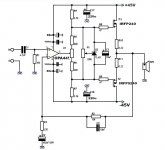
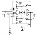
Hi to everybody
I realise thath I have found my limit in electronics.
I found on the net this simple schema thath arouse my curiosity, but at the same time I have reached a dead end.
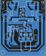
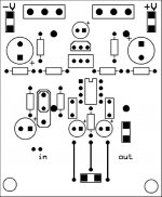
I dont know how to tune up an amplifier, I just dont know. Like I said before I'm a rookie, I am a dentist. I love to weld wires and components on the board since I was 13 , but theoretically speaking, sorry guys, it's too much for me. I have designed this PCB but I dont know is this good or bad.
If anybody reech to the point thath know how tune up the circuit, please let me know, I'll try to design the PCB, that is my limit.
Thanks to all of you, specially who answer topics in this thread.
Best regards
Braco Raab
I realise thath I have found my limit in electronics.
I found on the net this simple schema thath arouse my curiosity, but at the same time I have reached a dead end.
I dont know how to tune up an amplifier, I just dont know. Like I said before I'm a rookie, I am a dentist. I love to weld wires and components on the board since I was 13 , but theoretically speaking, sorry guys, it's too much for me. I have designed this PCB but I dont know is this good or bad.
If anybody reech to the point thath know how tune up the circuit, please let me know, I'll try to design the PCB, that is my limit.
Thanks to all of you, specially who answer topics in this thread.
Best regards
Braco Raab
hi bracoraab,
I like the original schematic better. I don't like the idea of a opamp outputting into a pot. I can't really offer a explaination, I just don't think a pot in the signal path is a good idea, a little DC offset is preferable.
Have you read the "Lightspeed Attenuator a new passive preamp" thread? George goes to great lengths to eliminate pots from the signal path.
http://www.diyaudio.com/forums/showthread.php?s=&threadid=80194&highlight=lightspeed
Anyway, I sure it will still work OK, maybe having the pot there is worth a few minutes thought. You could start off with a pot then replace it with a couple of resistors once the values are worked out.
regards
bracoraab: " ... I realise thath I have found my limit in electronics. ..."
Modern dentistry is a miracle of our age ... there is know way that I or most of us here would have a remote idea about the sophistication and technology of your profession ... it is certainly a completely different technology than electronics and DIY amp construction and design ...
I learned by building kits, starting with several old Heath Kits, then after years of practice and working as an electrician, got interested in the science and engineering behind it all ... and still learning. At your point in your electronics education, I would recommend as Greg says above, try building someone elses design and figure out what's going on there ... then graduate into rolling your own.
If you want to pursue your design further, do so, but don't put that much effort into the circuit board just yet ... better to make a breadboard model first and see and learn the hows and whys of "tuning it up" ...
Your progress so far is just Great with a capital G, the basic amp design is very viable and certainly worthwhile and with a little patience and some more work, it will sound very nice indeed. (Your design is very close to the recommendations of Texas Instruments' own ... so, yes it will work and work very well.)
Hi FastEddy
Mi first project that I build this year, was Mauro Penasa's project
http://www.diyaudio.com/forums/showthread.php?s=&threadid=54571&highlight=
First, I made a prototype, then I go to triamp my son's speakers with this project. Well, I made the boards of amplifier units and active crossovers, the only thing that I have to do, is assamble the whole sistem. That's why I'm searching for the next project (multiamp sistem to me). This "simple schema", is not my design, I found it in the internet, like I said before. I only can design a simple PSU by my own.
As you can see, my wish is to climb the "DIY Mountain" one step at the time. The mosfet sound, likes me, then I need a little help to know if the design is a success, or the resistor and caps values are fake.
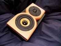
Here a picture of my little "baby" is the upper medium + tweeter baffle, I build it myself about two years ago.
Best regards
Braco Raab
Mi first project that I build this year, was Mauro Penasa's project
http://www.diyaudio.com/forums/showthread.php?s=&threadid=54571&highlight=
First, I made a prototype, then I go to triamp my son's speakers with this project. Well, I made the boards of amplifier units and active crossovers, the only thing that I have to do, is assamble the whole sistem. That's why I'm searching for the next project (multiamp sistem to me). This "simple schema", is not my design, I found it in the internet, like I said before. I only can design a simple PSU by my own.
As you can see, my wish is to climb the "DIY Mountain" one step at the time. The mosfet sound, likes me, then I need a little help to know if the design is a success, or the resistor and caps values are fake.
Here a picture of my little "baby" is the upper medium + tweeter baffle, I build it myself about two years ago.
Best regards
Braco Raab
Attachments
FastEddy said:
cs: " ... The OPA445 only has a gain-BW product of 2MHz, so the distortion at a closed loop gain of 30 may not be that good. This is why I used a closed loop gain of 2, then used another (lower voltage) op amp as a driver with a gain of 10-20 ..."
It may be a tossup as to which is lower distortion, phase shifting, noise contribution, etc., the added op-amp or having a higher gain on just the one op-amp.
Since the feedback is coming from the MOSFETs' (or transistors') output clear back to the input (negative on op-amp pin 2), the gain is for the total amp, not just the op-amp itself. In addition to R2, ... R5, R6, R8, R9, R10, R11 the DC offset pot and the impedence of the output transistors (or MOSFETs) all make a contribution to the overall gain / feedback loop, so the "real gain" at the op-amp is much less than 30 ... (My estimate is somewhere closer to an op-amp gain of 10 or 15 to 1 rather than the 30 to 1 of the whole amp ...)
The mosfet output stage will have a voltage gain just under unity, so the overall open-loop gain will be pretty much equal to that of the op amp alone. The closed loop gain is defined by the feedback resistors (10k and 330ohm, I think Baco was proposing ?), which would be 30 (about 29dB).
But as the op amp has a GBW product of 2MHz, you would have only 11dB of feedback at 20kHz, if the closed loop gain was 29dB. This may not be enough to reduce the mosfet distortion (unless they were run at high bias current current.
cs said:
But as the op amp has a GBW product of 2MHz, you would have only 11dB of feedback at 20kHz, if the closed loop gain was 29dB. This may not be enough to reduce the mosfet distortion (unless they were run at high bias current current.
Their are certain other techniques exist rather than using high feedback factor, high bias and so called error-correction to reduce distortion in vertical mosfets.....
- Status
- This old topic is closed. If you want to reopen this topic, contact a moderator using the "Report Post" button.
- Home
- Amplifiers
- Solid State
- Simple schema